- 您现在的位置:买卖IC网 > PDF目录64885 > FA7630CP 0.5 A DUAL SWITCHING CONTROLLER, 500 kHz SWITCHING FREQ-MAX, PDIP20 PDF资料下载
参数资料
| 型号: | FA7630CP |
| 元件分类: | 稳压器 |
| 英文描述: | 0.5 A DUAL SWITCHING CONTROLLER, 500 kHz SWITCHING FREQ-MAX, PDIP20 |
| 封装: | DIP-20 |
| 文件页数: | 1/5页 |
| 文件大小: | 61K |
| 代理商: | FA7630CP |
FA7630CP(E)
1
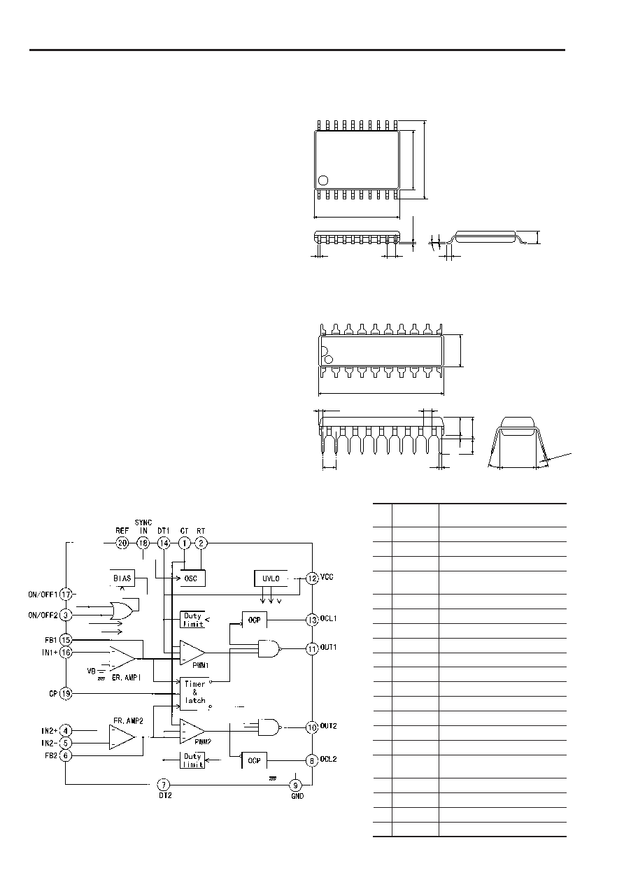
s Block diagram
Pin
Description
No.
symbol
1
CT
Oscillator timing capacitor
2
RT
Oscillator timing resistor
3
ON/OFF2 Output ON/OFF control 2
4
IN2+
Non-inverting input to error
amplifier
5
IN2–
Inverting input to error amplifier
6
FB2
Error amplifier output
7
DT2
Dead time adjustment
8
OCL2
Overcurrent limiting circuit 2
9
GND
Ground
10
OUT2
CH.2 output
11
OUT1
CH.1 output
12
VCC
Power supply
13
OCL1
Overcurrent limiting circuit
14
DT1
Dead time adjustment
15
FB1
Error amplifier output
16
IN1+
Non-inverting input to error
amplifier
17
ON/OFF1 Output ON/OFF control 1
18
SYNC IN
Synchronizing signal input
19
CP
Timer and latch circuit
20
REF
Reference voltage output
FA7630CP(E)
s Dimensions, mm
SSOP-20
1
7.2
10
11
20
5.3
0.6
0~10
0.65
7.9
±0.3
0.1
±0.1
0.3
0.2
+
0
.1
–0
.05
2.1max
DIP-20
1
20
11
10
24.4
6.4
7.62
3.6
5.1max
1.52
0.77
2.54min
0.51min
0~15
0.46±0.1
2.54±0.25
0.25
+0.1
–0.05
Bipolar IC
For Switching Power Supply Control
s Description
The FA7630CP(E) is dual channel PWM-type switching power
supply control IC.
This IC can drive Pch-MOSFET directly and is optimum for
large power DC-DC converter.
This IC has all the necessary protection functions for a power
MOSFET. It is optimum for a portable equipment power
supply which uses low-voltage input to output comparably
large power.
s Features
Dual channel PWM-type switching power supply control
±2.6% (VREF) and ±3% (VB) reference voltage
Low voltage operation (Vcc: 5 to 20V)
Drive circuit for connecting a Pch-MOSFET
Overload cutoff circuit with timer latch circuit
Soft start circuit
Undervoltage lockout function (UVLO)
Pulse-by-pulse overcurrent limiting function
Output ON/OFF control function for each channel
Master-slave synchronized operation without external
components
Maximum operating frequency is 500kHz
相关PDF资料 |
PDF描述 |
|---|---|
| FA7630CE | 0.5 A DUAL SWITCHING CONTROLLER, 500 kHz SWITCHING FREQ-MAX, PDSO20 |
| FA7630M | DUAL SWITCHING CONTROLLER, 500 kHz SWITCHING FREQ-MAX, PDSO20 |
| FAN4822IN_NL | 0.5 A POWER FACTOR CONTROLLER, PDIP14 |
| FAN4822IP | 0.5 A POWER FACTOR CONTROLLER, PDIP14 |
| FAN4822IS | 0.5 A POWER FACTOR CONTROLLER, PDSO16 |
相关代理商/技术参数 |
参数描述 |
|---|---|
| FA7630CPE | 制造商:FUJI 制造商全称:Fuji Electric 功能描述:Bipolar IC For Switching Power Supply Control |
| FA765 | 制造商:Black Box Corporation 功能描述:MMJ Modular Adapter Kit, DB9 to MMJ, Male |
| FA766 | 制造商:Black Box Corporation 功能描述:COMPUTER ACCESSORY |
| FA76AXPM1 | 制造商:Carling Technologies 功能描述:F-Series Toggle Switch |
| FA76A-XPM1 | 制造商:Carling Technologies 功能描述:F-SERIES TOGGLE SWITCH - Bulk |
发布紧急采购,3分钟左右您将得到回复。