- 您现在的位置:买卖IC网 > PDF目录299040 > FAN1581P FETs - Nch 250V<VDSS=500V; ; Package: TO-3P(L); R DS On (Ω): (max 0.11); P D (W): (max 50) PDF资料下载
参数资料
| 型号: | FAN1581P |
| 英文描述: | FETs - Nch 250V<VDSS=500V; ; Package: TO-3P(L); R DS On (Ω): (max 0.11); P D (W): (max 50) |
| 中文描述: | 积极可调电压稳压器 |
| 文件页数: | 8/11页 |
| 文件大小: | 106K |
| 代理商: | FAN1581P |
FAN1581
PRODUCT SPECIFICATION
6
REV. 1.0.2 8/15/01
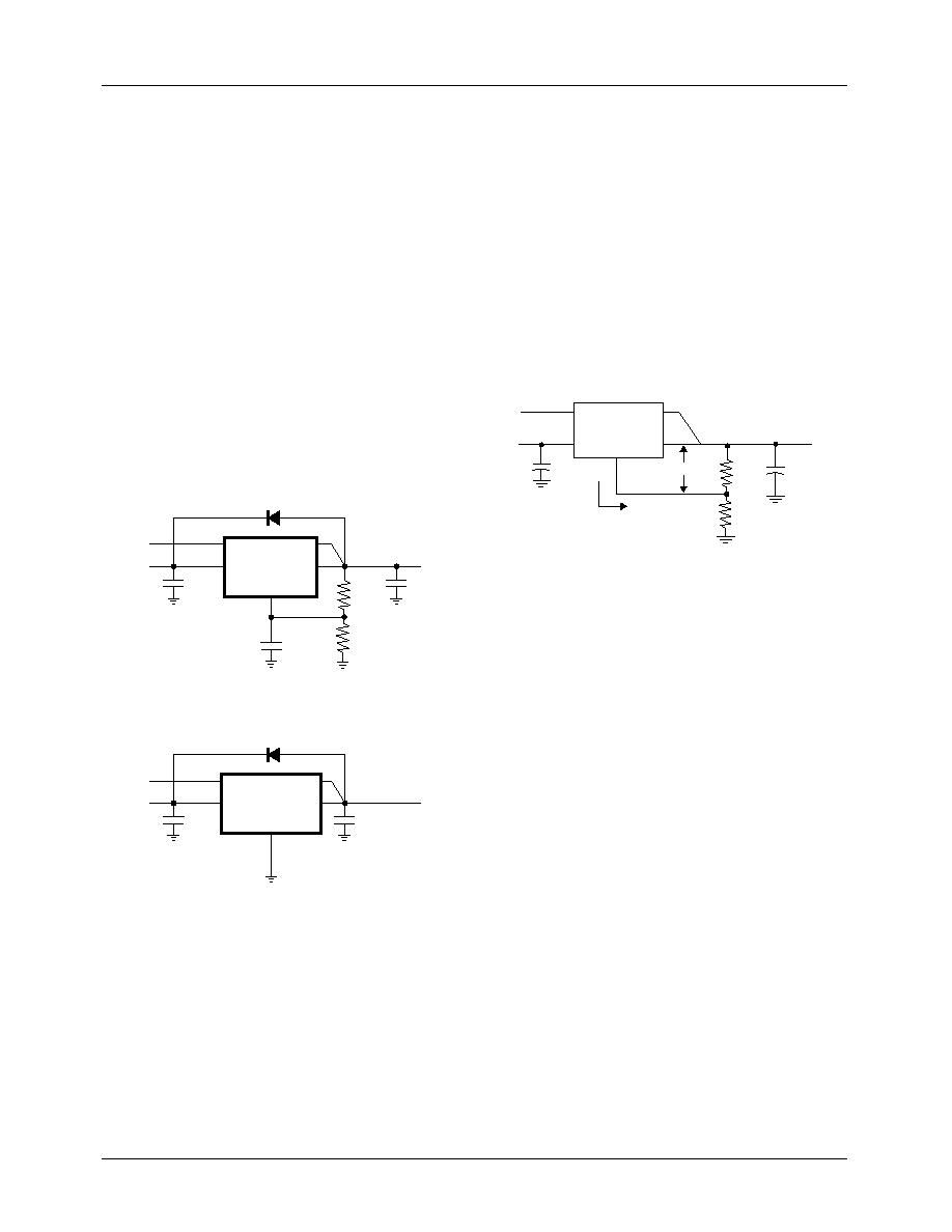
A protection diode between the input and output pins is usu-
ally not needed. An internal diode between the input and the
output pins on the FAN1581 series can handle microsecond
surge currents of 50A to 100A. Even with large value output
capacitors it is difcult to obtain those values of surge cur-
rents in normal operation. Only with large values of output
capacitance, such as 1000F to 5000F, and with the input
pin instantaneously shorted to ground can damage occur. A
crowbar circuit at the input can generate those levels of current;
a diode from output to input is then recommended, as shown
in Figure 1. Usually, normal power supply cycling or system
“hot plugging and unplugging” will not generate current
large enough to do any damage.
The adjust pin can be driven on a transient basis ±7V with
respect to the output, without any device degradation. As with
any IC regulator, exceeding the maximum input-to-output
voltage differential causes the internal transistors to break
down and none of the protection circuitry is then functional.
Figure 1. Optional Protection Diode
Ripple Rejection
In applications that require improved ripple rejection, a bypass
capacitor from the adjust pin of the FAN1581 to ground
reduces the output ripple by the ratio of VOUT/1.25V. The
impedance of the adjust pin capacitor at the ripple frequency
should be less than the value of R1 (typically in the range of
100
to 120) in the feedback divider network in Figure 1.
Therefore, the value of the required adjust pin capacitor is a
function of the input ripple frequency. For example, if R1 equals
100
and the ripple frequency equals 120Hz, the adjust pin
capacitor should be 22F. At 10kHz, only 0.22F is needed.
Output Voltage
The FAN1581 regulator develops a 1.25V reference voltage
between the output pin and the adjust pin (see Figure 2).
Placing a resistor R1 between these two terminals causes a
constant current to ow through R1 and down through R2 to
set the overall output voltage. Normally, this current is the
specied minimum load current of 10mA.
The current out of the adjust pin adds to the current from R1
and is typically 50A. Its output voltage contribution is
small and only needs consideration when a very precise out-
put voltage setting is required.
Figure 2. Basic Regulator Circuit
Load Regulation
The FAN1581 family provides true remote sensing, eliminat-
ing output voltage errors due to trace resistance. To utilize
remote sensing, connect the VSENSE pin directly to the
load, rather than at the VOUT pin. If the load is more than 1"
away from the FAN1581, it may be necessary to increase the
load capacitance to ensure stability.
Thermal Considerations
The FAN1581 series protect themselves under overload con-
ditions with internal power and thermal limiting circuitry.
However, for normal continuous load conditions, do not exceed
maximum junction temperature ratings. It is important to
consider all sources of thermal resistance from junction-to-
ambient. These sources include the junction-to-case resistance,
the case-to-heat sink interface resistance, and the heat sink
resistance. Thermal resistance specications have been
developed to more accurately reect device temperature and
ensure safe operating temperatures. The electrical character-
istics section provides a separate thermal resistance and
maximum junction temperature for both the control circuitry
and the power transistor. Calculate the maximum junction
temperature for both sections to ensure that both thermal
limits are met.
For example, look at using an FAN1581M-1.5 to generate
5A @ 1.5V ± 2% from a 3.3V source (3.2V to 3.6V).
FAN1581
Adj
C2
22
F
VOUT
+
C1
10
F
+
CADJ
+
Vcntl
Vsense
Vin
Vout
R1
R2
D1
1N4002
(OPTIONAL)
VIN
VOUT
FAN1581–1.5, 2.5
Gnd
C2
22
F
VOUT
+
C1
10
F
+
Vcntl
Vsense
Vin
Vout
D1
1N4002
(OPTIONAL)
VIN
VCNTL
C2
22
F
VIN
VOUT
VREF
C1
10
F
Vcntl
+
Vcntl
Vsense
Vin
Adj Vout
FAN1581
R1
R2
IADJ
50
A
VOUT = VREF (1+R2/R1) + IADJ (R2)
相关PDF资料 |
PDF描述 |
|---|---|
| FAN1581P-1.5 | FETs - Nch 250V<VDSS=500V; Surface Mount Type: N/Y; Package: TO-220FL/SM; R DS On (Ω): (max 0.65); P D (W): (max 10) |
| FAN1581P15X | FETs - Nch 250V<VDSS=500V; Surface Mount Type: N; Package: TO-220NIS; R DS On (Ω): (max 0.62); P D (W): (max 12) |
| FAN1581P-2.5 | FETs - Nch 250V<VDSS=500V; Surface Mount Type: N; Package: TO-220NIS; R DS On (Ω): (max 1.8); P D (W): (max 5) |
| FAN1581P25X | FETs - Nch 250V<VDSS=500V; ; Package: TPS; R DS On (Ω): (max 4.6); P D (W): (max 1) |
| FAN1581PX | FETs - Nch 250V<VDSS=500V; Surface Mount Type: N/Y; Package: TO-220FL/SM; R DS On (Ω): (max 0.4); P D (W): (max 13) |
相关代理商/技术参数 |
参数描述 |
|---|---|
| FAN1581P-1.5 | 制造商:未知厂家 制造商全称:未知厂家 功能描述:Positive Fixed Voltage Regulator |
| FAN1581P15X | 制造商:未知厂家 制造商全称:未知厂家 功能描述:VOLT REGULATOR|FIXED|+1.5V|BIPOLAR|SIP|5PIN|PLASTIC |
| FAN1581P-2.5 | 制造商:未知厂家 制造商全称:未知厂家 功能描述:Positive Fixed Voltage Regulator |
| FAN1581P25X | 制造商:未知厂家 制造商全称:未知厂家 功能描述:VOLT REGULATOR|FIXED|+2.5V|BIPOLAR|SIP|5PIN|PLASTIC |
| FAN1581PX | 制造商:未知厂家 制造商全称:未知厂家 功能描述:VOLT REGULATOR|ADJUSTABLE|+1.25 TO +5V|BIPOLAR|SIP|5PIN|PLASTIC |
发布紧急采购,3分钟左右您将得到回复。