- 您现在的位置:买卖IC网 > PDF目录172369 > FAN2013BMPX (FAIRCHILD SEMICONDUCTOR CORP) PDF资料下载
参数资料
| 型号: | FAN2013BMPX |
| 厂商: | FAIRCHILD SEMICONDUCTOR CORP |
| 元件分类: | 稳压器 |
| 中文描述: | SWITCHING REGULATOR, PDSO6 |
| 封装: | 3 X 3 MM, GREEN, MO-229WEEA, MLP-6 |
| 文件页数: | 3/9页 |
| 文件大小: | 532K |
| 代理商: | FAN2013BMPX |
2008 Fairchild Semiconductor Corporation
www.fairchildsemi.com
FAN2013B Rev. 1.0.1
3
FAN2013B
—
2A
Low-Voltage,
Current-M
ode
Synchronous
PWM
Buck
Regulator
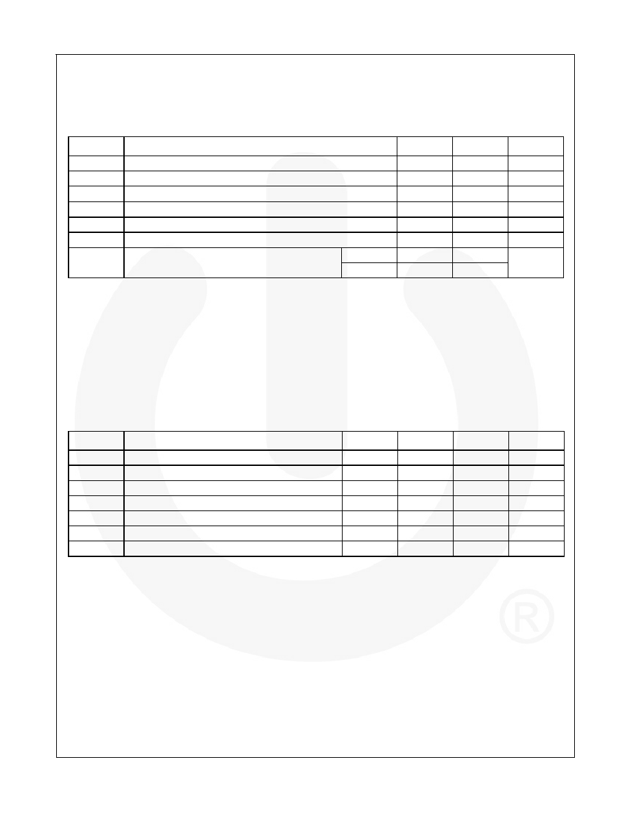
Absolute Maximum Ratings
Stresses exceeding the absolute maximum ratings may damage the device. The device may not function or be
operable above the recommended operating conditions and stressing the parts to these levels is not recommended.
In addition, extended exposure to stresses above the recommended operating conditions may affect device
reliability. The absolute maximum ratings are stress ratings only.
Symbol
Parameter
Min.
Max.
Unit
VIN
Supply Voltage
-0.3
7.0
V
Input Voltage on PVIN and Any Other Pin
-0.3
VIN
V
θJC
Thermal Resistance, Junction-to-Tab
(1)
8
°C/W
TL
Lead Soldering Temperature (10 Seconds)
+260
°C
TSTG
Storage Temperature
-65
+150
°C
TJ
Junction Temperature
-40
+150
°C
ESD
Electrostatic Discharge Protection Level
(2)
HBM
3.5
kV
CDM
2.0
Notes:
1.
Junction-to-ambient thermal resistance,
θJA, is a strong function of PCB material, board thickness, thickness and
number of copper planes, number of via used, diameter of via used, available copper surface, and attached heat
sink characteristics.
2.
Using Mil Std. 883E, method 3015.7 (Human Body Model) and EIA/JESD22C101-A (Charged Device Model).
Recommended Operating Conditions
The Recommended Operating Conditions table defines the conditions for actual device operation. Recommended
operating conditions are specified to ensure optimal performance to the datasheet specifications. Fairchild does not
recommend exceeding them or designing to Absolute Maximum Ratings.
Symbols
Parameter
Min.
Typ.
Max.
Unit
VIN
Supply Voltage Range
4.5
5.5
V
VOUT
Output Voltage Range, Adjustable Version
0.8
3.6
V
IOUT
Output Current
2.0
A
L
Inductor
(3)
2.2
H
CIN
Input Capacitor
(3)
10
20
F
COUT
Output Capacitor
(3)
20
40
F
TA
Operating Ambient Temperature Range
-40
+85
°C
Note:
3.
Refer to the Applications section for details
.
相关PDF资料 |
PDF描述 |
|---|---|
| FAN5092MTC | |
| FAN5094MTC | |
| FAN5341UMPX | |
| FAN5353MPX | |
| FAN5354MPX | |
相关代理商/技术参数 |
参数描述 |
|---|---|
| FAN2013MPX | 功能描述:直流/直流开关转换器 PWM Buck Regulator Standard Switch RoHS:否 制造商:STMicroelectronics 最大输入电压:4.5 V 开关频率:1.5 MHz 输出电压:4.6 V 输出电流:250 mA 输出端数量:2 最大工作温度:+ 85 C 安装风格:SMD/SMT |
| FAN20LV03MPX | 制造商:Fairchild Semiconductor Corporation 功能描述: |
| FAN2103 | 制造商:FAIRCHILD 制造商全称:Fairchild Semiconductor 功能描述:TinyBuck⑩ 3A, 24V Input, Integrated Synchronous Buck Regulator |
| FAN2103_08 | 制造商:FAIRCHILD 制造商全称:Fairchild Semiconductor 功能描述:TinyBuck⑩ 3A, 24V Input, Integrated Synchronous Buck Regulator |
| FAN2103_12 | 制造商:FAIRCHILD 制造商全称:Fairchild Semiconductor 功能描述:3 A, 24 V Input, Integrated Synchronous Buck Regulator |
发布紧急采购,3分钟左右您将得到回复。