- 您现在的位置:买卖IC网 > PDF目录17514 > FAN3225TMX (Fairchild Semiconductor)IC GATE DRIVER DUAL 4A 8-SOIC PDF资料下载
参数资料
| 型号: | FAN3225TMX |
| 厂商: | Fairchild Semiconductor |
| 文件页数: | 19/27页 |
| 文件大小: | 0K |
| 描述: | IC GATE DRIVER DUAL 4A 8-SOIC |
| 标准包装: | 1 |
| 配置: | 低端 |
| 输入类型: | 反相和非反相 |
| 延迟时间: | 17ns |
| 电流 - 峰: | 5A |
| 配置数: | 2 |
| 输出数: | 2 |
| 电源电压: | 4.5 V ~ 18 V |
| 工作温度: | -40°C ~ 125°C |
| 安装类型: | 表面贴装 |
| 封装/外壳: | 8-SOIC(0.154",3.90mm 宽) |
| 供应商设备封装: | 8-SOIC |
| 包装: | 标准包装 |
| 其它名称: | FAN3225TMXDKR |
第1页第2页第3页第4页第5页第6页第7页第8页第9页第10页第11页第12页第13页第14页第15页第16页第17页第18页当前第19页第20页第21页第22页第23页第24页第25页第26页第27页
�� �
�
�Applications� Information�
�Input� Thresholds�
�Each� member� of� the� FAN322x� driver� family� consists� of�
�two� identical� channels� that� may� be� used� independently�
�at� rated� current� or� connected� in� parallel� to� double� the�
�individual� current� capacity.� In� the� FAN3223� and�
�FAN3224,� channels� A� and� B� can� be� enabled� or� disabled�
�independently� using� ENA� or� ENB,� respectively.� The� EN�
�pin� has� TTL� thresholds� for� parts� with� either� CMOS� or�
�TTL� input� thresholds.� If� ENA� and� ENB� are� not�
�connected,� an� internal� pull-up� resistor� enables� the� driver�
�channels� by� default.� ENA� and� ENB� have� TTL� thresholds�
�in� parts� with� either� TTL� or� CMOS� INx� threshold.� If� the�
�channel� A� and� channel� B� inputs� and� outputs� are�
�connected� in� parallel� to� increase� the� driver� current�
�capacity,� ENA� and� ENB� should� be� connected� and�
�driven� together.�
�The� FAN322x� family� offers� versions� in� either� TTL� or�
�CMOS� input� thresholds.� In� the� FAN322xT,� the� input�
�thresholds� meet� industry-standard� TTL-logic� thresholds�
�independent� of� the� V� DD� voltage,� and� there� is� a�
�hysteresis� voltage� of� approximately� 0.4� V.� These� levels�
�permit� the� inputs� to� be� driven� from� a� range� of� input� logic�
�signal� levels� for� which� a� voltage� over� 2� V� is� considered�
�logic� HIGH.� The� driving� signal� for� the� TTL� inputs� should�
�have� fast� rising� and� falling� edges� with� a� slew� rate� of�
�6� V/μs� or� faster,� so� a� rise� time� from� 0� to� 3.3� V� should� be�
�550� ns� or� less.� With� reduced� slew� rate,� circuit� noise�
�could� cause� the� driver� input� voltage� to� exceed� the�
�hysteresis� voltage� and� retrigger� the� driver� input,� causing�
�erratic� operation.�
�In� the� FAN322xC,� the� logic� input� thresholds� are�
�dependent� on� the� V� DD� level� and,� with� V� DD� of� 12V,� the�
�logic� rising� edge� threshold� is� approximately� 55%� of� V� DD�
�and� the� input� falling� edge� threshold� is� approximately�
�38%� of� V� DD� .� The� CMOS� input� configuration� offers� a�
�hysteresis� voltage� of� approximately� 17%� of� V� DD� .� The�
�CMOS� inputs� can� be� used� with� relatively� slow� edges�
�(approaching� DC)� if� good� decoupling� and� bypass�
�techniques� are� incorporated� in� the� system� design� to�
�prevent� noise� from� violating� the� input� voltage� hysteresis�
�window.� This� allows� setting� precise� timing� intervals� by�
�fitting� an� R-C� circuit� between� the� controlling� signal� and�
�the� IN� pin� of� the� driver.� The� slow� rising� edge� at� the� IN�
�pin� of� the� driver� introduces� a� delay� between� the�
�controlling� signal� and� the� OUT� pin� of� the� driver.�
�Static� Supply� Current�
�In� the� I� DD� (static)� typical� performance� characteristics�
�(Figure� 12� -� Figure� 14� and� Figure� 19� -� Figure� 21)� ,� the�
�curve� is� produced� with� all� inputs/enables� floating� (OUT�
�is� low)� and� indicates� the� lowest� static� I� DD� current� for� the�
�tested� configuration.� For� other� states,� additional� current�
�flows� through� the� 100� k� ?� resistors� on� the� inputs� and�
�outputs� shown� in� the� block� diagram� of� each� part� (see�
�Figure� 5� -� Figure� 7)� .� In� these� cases,� the� actual� static� I� DD�
�current� is� the� value� obtained� from� the� curves� plus� this�
�additional� current.�
�?� 2007� Fairchild� Semiconductor� Corporation�
�FAN3223� /� FAN3224� /� FAN3225� ?� Rev.� 1.1.4�
�19�
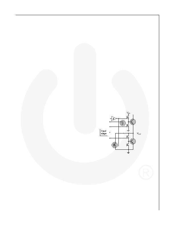
�MillerDrive?� Gate� Drive� Technology�
�FAN322x� gate� drivers� incorporate� the� MillerDrive?�
�architecture� shown� in� Figure� 47.� For� the� output� stage,� a�
�combination� of� bipolar� and� MOS� devices� provide� large�
�currents� over� a� wide� range� of� supply� voltage� and�
�temperature� variations.� The� bipolar� devices� carry� the�
�bulk� of� the� current� as� OUT� swings� between� 1/3� to� 2/3�
�V� DD� and� the� MOS� devices� pull� the� output� to� the� HIGH� or�
�LOW� rail.�
�The� purpose� of� the� MillerDrive?� architecture� is� to�
�speed� up� switching� by� providing� high� current� during� the�
�Miller� plateau� region� when� the� gate-drain� capacitance� of�
�the� MOSFET� is� being� charged� or� discharged� as� part� of�
�the� turn-on� /� turn-off� process.�
�For� applications� that� have� zero� voltage� switching� during�
�the� MOSFET� turn-on� or� turn-off� interval,� the� driver�
�supplies� high� peak� current� for� fast� switching� even�
�though� the� Miller� plateau� is� not� present.� This� situation�
�often� occurs� in� synchronous� rectifier� applications�
�because� the� body� diode� is� generally� conducting� before�
�the� MOSFET� is� switched� ON.�
�The� output� pin� slew� rate� is� determined� by� V� DD� voltage�
�and� the� load� on� the� output.� It� is� not� user� adjustable,� but�
�a� series� resistor� can� be� added� if� a� slower� rise� or� fall� time�
�at� the� MOSFET� gate� is� needed.�
�Figure� 47.� MillerDrive?� Output� Architecture�
�Under-Voltage� Lockout�
�The� FAN322x� startup� logic� is� optimized� to� drive� ground-�
�referenced� N-channel� MOSFETs� with� an� under-voltage�
�lockout� (UVLO)� function� to� ensure� that� the� IC� starts� up�
�in� an� orderly� fashion.� When� V� DD� is� rising,� yet� below� the�
�3.9� V� operational� level,� this� circuit� holds� the� output�
�LOW,� regardless� of� the� status� of� the� input� pins.� After� the�
�part� is� active,� the� supply� voltage� must� drop� 0.2� V� before�
�the� part� shuts� down.� This� hysteresis� helps� prevent�
�chatter� when� low� V� DD� supply� voltages� have� noise� from�
�the� power� switching.� This� configuration� is� not� suitable�
�for� driving� high-side� P-channel� MOSFETs� because� the�
�low� output� voltage� of� the� driver� would� turn� the� P-channel�
�MOSFET� ON� with� V� DD� below� 3.9� V.�
�www.fairchildsemi.com�
�相关PDF资料 |
PDF描述 |
|---|---|
| T95S224M035LZSL | CAP TANT 0.22UF 35V 20% 1507 |
| HC49US-14.7456MABJ-UB | CRYSTAL 14.7456 MHZ 18PF HC49/US |
| HC49US-4.000MABJ-UB | CRYSTAL 4.000 MHZ 18PF HC49/US |
| GCC08DRTS-S13 | CONN EDGECARD 16POS .100 EXTEND |
| HC49US-28.224MABJ-UB | CRYSTAL 28.224 MHZ 18PF HC49/US |
相关代理商/技术参数 |
参数描述 |
|---|---|
| FAN3225TMX_12 | 制造商:FAIRCHILD 制造商全称:Fairchild Semiconductor 功能描述:Dual 4A High-Speed, Low-Side Gate Drivers |
| FAN3226 | 制造商:FAIRCHILD 制造商全称:Fairchild Semiconductor 功能描述:Dual 2A High-Speed, Low-Side Gate Drivers |
| FAN3226_10 | 制造商:FAIRCHILD 制造商全称:Fairchild Semiconductor 功能描述:Dual 2A High-Speed, Low-Side Gate Drivers |
| FAN3226_11 | 制造商:FAIRCHILD 制造商全称:Fairchild Semiconductor 功能描述:Dual 2A High-Speed, Low-Side Gate Drivers |
| FAN3226_12 | 制造商:FAIRCHILD 制造商全称:Fairchild Semiconductor 功能描述:Dual 2A High-Speed, Low-Side Gate Drivers |
发布紧急采购,3分钟左右您将得到回复。