- 您现在的位置:买卖IC网 > PDF目录17289 > FAN3227CMX (Fairchild Semiconductor)IC GATE DVR DUAL 2A 8-SOIC PDF资料下载
参数资料
| 型号: | FAN3227CMX |
| 厂商: | Fairchild Semiconductor |
| 文件页数: | 19/26页 |
| 文件大小: | 0K |
| 描述: | IC GATE DVR DUAL 2A 8-SOIC |
| 标准包装: | 1 |
| 配置: | 低端 |
| 输入类型: | 非反相 |
| 延迟时间: | 15ns |
| 电流 - 峰: | 3A |
| 配置数: | 2 |
| 输出数: | 2 |
| 电源电压: | 4.5 V ~ 18 V |
| 工作温度: | -40°C ~ 125°C |
| 安装类型: | 表面贴装 |
| 封装/外壳: | 8-SOIC(0.154",3.90mm 宽) |
| 供应商设备封装: | 8-SOIC |
| 包装: | 标准包装 |
| 产品目录页面: | 1215 (CN2011-ZH PDF) |
| 其它名称: | FAN3227CMXDKR |
�� �
�
�V� DD� Bypass� Capacitor� Guidelines�
�To� enable� this� IC� to� turn� a� device� on� quickly,� a� local� high-�
�frequency� bypass� capacitor� C� BYP� with� low� ESR� and� ESL�
�should� be� connected� between� the� VDD� and� GND� pins�
�with� minimal� trace� length.� This� capacitor� is� in� addition� to�
�bulk� electrolytic� capacitance� of� 10� μF� to� 47� μF� commonly�
�found� on� driver� and� controller� bias� circuits.�
�A� typical� criterion� for� choosing� the� value� of� C� BYP� is� to�
�keep� the� ripple� voltage� on� the� V� DD� supply� to� ≤� 5%.� This�
�is� often� achieved� with� a� value� ≥� 20� times� the� equivalent�
�load� capacitance� C� EQV� ,� defined� here� as� Q� GATE� /V� DD� .�
�Ceramic� capacitors� of� 0.1� μF� to� 1� μF� or� larger� are�
�common� choices,� as� are� dielectrics,� such� as� X5R� and�
�X7R� with� good� temperature� characteristics� and� high�
�pulse� current� capability.�
�If� circuit� noise� affects� normal� operation,� the� value� of�
�C� BYP� may� be� increased� to� 50-100� times� the� C� EQV� ,� or�
�C� BYP� may� be� split� into� two� capacitors.� One� should� be� a�
�larger� value,� based� on� equivalent� load� capacitance,� and�
�the� other� a� smaller� value,� such� as� 1-10� nF� mounted�
�closest� to� the� VDD� and� GND� pins� to� carry� the� higher�
�best� results,� make� connections� to� all� pins� as� short�
�and� direct� as� possible.�
�?� The� FAN322x� is� compatible� with� many� other�
�industry-standard� drivers.� In� single� input� parts� with�
�enable� pins,� there� is� an� internal� 100� k� Ω� resistor� tied�
�to� V� DD� to� enable� the� driver� by� default;� this� should� be�
�considered� in� the� PCB� layout.�
�?� The� turn-on� and� turn-off� current� paths� should� be�
�minimized,� as� discussed� in� the� following� section.�
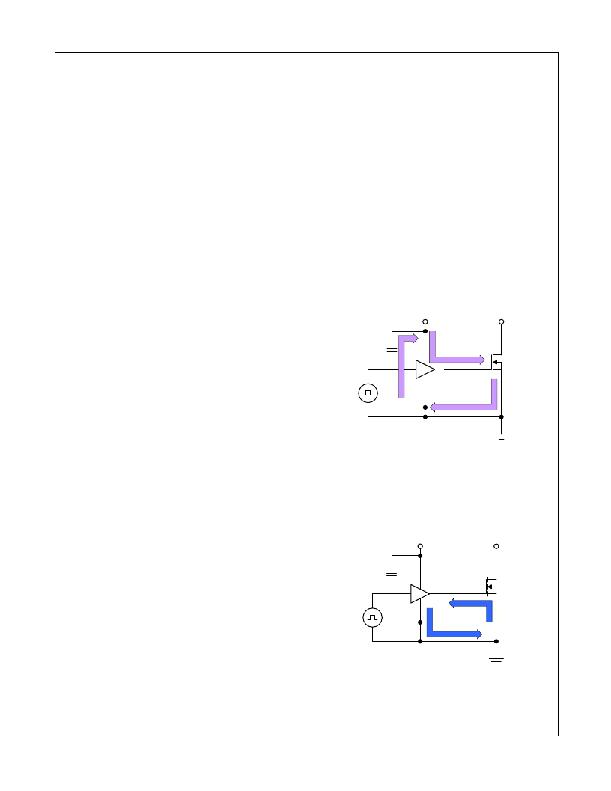
�Figure� 49� shows� the� pulsed� gate� drive� current� path�
�when� the� gate� driver� is� supplying� gate� charge� to� turn� the�
�MOSFET� on.� The� current� is� supplied� from� the� local�
�bypass� capacitor,� C� BYP� ,� and� flows� through� the� driver� to�
�the� MOSFET� gate� and� to� ground.� To� reach� the� high�
�peak� currents� possible,� the� resistance� and� inductance� in�
�the� path� should� be� minimized.� The� localized� C� BYP� acts�
�to� contain� the� high� peak� current� pulses� within� this� driver-�
�MOSFET� circuit,� preventing� them� from� disturbing� the�
�sensitive� analog� circuitry� in� the� PWM� controller.�
�frequency� components� of� the� current� pulses.� The�
�bypass� capacitor� must� provide� the� pulsed� current� from�
�both� of� the� driver� channels� and,� if� the� drivers� are�
�switching� simultaneously,� the� combined� peak� current�
�sourced� from� the� C� BYP� would� be� twice� as� large� as� when�
�a� single� channel� is� switching.�
�Layout� and� Connection� Guidelines�
�The� FAN3226-26� family� of� gate� drivers� incorporates�
�fast-reacting� input� circuits,� short� propagation� delays,�
�and� powerful� output� stages� capable� of� delivering� current�
�peaks� over� 2� A� to� facilitate� voltage� transition� times� from�
�under� 10� ns� to� over� 150� ns.� The� following� layout� and�
�connection� guidelines� are� strongly� recommended:�
�PWM�
�C� BYP�
�V� DD�
�FAN322x�
�V� DS�
�?�
�?�
�?�
�?�
�Keep� high-current� output� and� power� ground� paths�
�separate� logic� and� enable� input� signals� and� signal�
�ground� paths.� This� is� especially� critical� when�
�dealing� with� TTL-level� logic� thresholds� at� driver�
�inputs� and� enable� pins.�
�Keep� the� driver� as� close� to� the� load� as� possible� to�
�minimize� the� length� of� high-current� traces.� This�
�reduces� the� series� inductance� to� improve� high-�
�speed� switching,� while� reducing� the� loop� area� that�
�can� radiate� EMI� to� the� driver� inputs� and�
�surrounding� circuitry.�
�If� the� inputs� to� a� channel� are� not� externally�
�connected,� the� internal� 100� k� Ω� resistors� indicated�
�on� block� diagrams� command� a� low� output.� In� noisy�
�environments,� it� may� be� necessary� to� tie� inputs� of�
�an� unused� channel� to� VDD� or� GND� using� short�
�traces� to� prevent� noise� from� causing� spurious�
�output� switching.�
�Many� high-speed� power� circuits� can� be� susceptible�
�to� noise� injected� from� their� own� output� or� other�
�external� sources,� possibly� causing� output� re-�
�triggering.� These� effects� can� be� obvious� if� the�
�circuit� is� tested� in� breadboard� or� non-optimal� circuit�
�layouts� with� long� input,� enable,� or� output� leads.� For�
�Figure� 49.� Current� Path� for� MOSFET� Turn-on�
�Figure� 50� shows� the� current� path� when� the� gate� driver�
�turns� the� MOSFET� off.� Ideally,� the� driver� shunts� the�
�current� directly� to� the� source� of� the� MOSFET� in� a� small�
�circuit� loop.� For� fast� turn-off� times,� the� resistance� and�
�inductance� in� this� path� should� be� minimized.�
�V� DD� V� DS�
�C� BYP�
�FAN322x�
�PWM�
�Figure� 50.� Current� Path� for� MOSFET� Turn-off�
�?� 2007� Fairchild� Semiconductor� Corporation�
�FAN3226� /� FAN3227� /� FAN3228� /� FAN3229� ?� Rev.� 1.1.0�
�19�
�www.fairchildsemi.com�
�相关PDF资料 |
PDF描述 |
|---|---|
| GBM10DCCN-S189 | CONN EDGECARD 20POS R/A .156 SLD |
| TH3D226K025A0600 | CAP TANT 22UF 25V 10% 2917 |
| GBM10DCCH-S189 | CONN EDGECARD 20POS R/A .156 SLD |
| ISL6266AEVAL1Z | EVAL BOARD 1 FOR ISL6266A |
| 0210490779 | CABLE JUMPER 1.25MM .178M 9POS |
相关代理商/技术参数 |
参数描述 |
|---|---|
| FAN3227CMX_12 | 制造商:FAIRCHILD 制造商全称:Fairchild Semiconductor 功能描述:Dual 2A High-Speed, Low-Side Gate Drivers |
| FAN3227CMX_F085 | 功能描述:功率驱动器IC Dual 2A L-Side Drvr RoHS:否 制造商:Micrel 产品:MOSFET Gate Drivers 类型:Low Cost High or Low Side MOSFET Driver 上升时间: 下降时间: 电源电压-最大:30 V 电源电压-最小:2.75 V 电源电流: 最大功率耗散: 最大工作温度:+ 85 C 安装风格:SMD/SMT 封装 / 箱体:SOIC-8 封装:Tube |
| FAN3227T | 制造商:FAIRCHILD 制造商全称:Fairchild Semiconductor 功能描述:2A Low-Voltage PMOS-NMOS Bridge Driver |
| FAN3227TMPX | 功能描述:功率驱动器IC Dual 2A High-Speed Low-Side Gate RoHS:否 制造商:Micrel 产品:MOSFET Gate Drivers 类型:Low Cost High or Low Side MOSFET Driver 上升时间: 下降时间: 电源电压-最大:30 V 电源电压-最小:2.75 V 电源电流: 最大功率耗散: 最大工作温度:+ 85 C 安装风格:SMD/SMT 封装 / 箱体:SOIC-8 封装:Tube |
| FAN3227TMX | 功能描述:功率驱动器IC dual 2A with non-inverting TTL RoHS:否 制造商:Micrel 产品:MOSFET Gate Drivers 类型:Low Cost High or Low Side MOSFET Driver 上升时间: 下降时间: 电源电压-最大:30 V 电源电压-最小:2.75 V 电源电流: 最大功率耗散: 最大工作温度:+ 85 C 安装风格:SMD/SMT 封装 / 箱体:SOIC-8 封装:Tube |
发布紧急采购,3分钟左右您将得到回复。