- 您现在的位置:买卖IC网 > PDF目录370147 > FAN4272MA Voltage-Feedback Operational Amplifier PDF资料下载
参数资料
| 型号: | FAN4272MA |
| 英文描述: | Voltage-Feedback Operational Amplifier |
| 中文描述: | 电压反馈运算放大器 |
| 文件页数: | 2/10页 |
| 文件大小: | 196K |
| 代理商: | FAN4272MA |
lead temperature (10 sec)
+260
°
C
operating temperature range (recommended)
-40
°
C to +125
°
C
input voltage range
+V
s
+ 0.5V, -V
s
- 0.5V
DATA SHEET
FAN4272
2
Preliminary September 2001
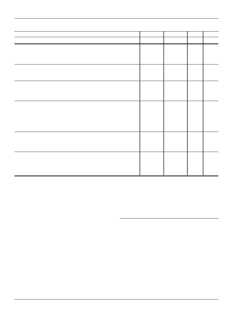
Parameters
Case Temperature
Conditions
TYP
+25
°
C
Min & Max
+25
°
C
UNITS
NOTES
Frequency Domain Response
-3dB bandwidth
G = +1, Vo= 0.02V
pp
G = +2, Vo= 0.2V
pp
G = +2, Vo= 2V
pp
4.9
3.7
1.4
2.2
MHz
MHz
MHz
MHz
1
full power bandwidth
gain bandwidth product
Time Domain Response
rise and fall time
overshoot
slew rate
Distortion and Noise Response
2nd harmonic distortion
3rd harmonic distortion
THD
input voltage noise
DC Performance
input offset voltage
average drift
input bias current
average drift
power supply rejection ratio
open loop gain
quiescent current per channel
1V step
1V step
1V step
163
<1
5.3
ns
%
V/
μ
s
1V
pp
, 10kHz
1V
pp
, 10kHz
1V
pp
, 10kHz
>10kHz
-72
-72
0.03
26
dBc
dBc
%
nV/
√
Hz
0.5
4
90
32
83
90
136
mV
μ
V/
°
C
nA
pA/
°
C
dB
dB
μ
A
DC
R
L
= 10k
Input Characteristics
input resistance
input capacitance
input common mode voltage range
common mode rejection ratio
Output Characteristics
output voltage swing
12
2
M
pF
V
dB
-0.25 to 2.95
81
DC, V
cm
= 0V to V
s
R
L
= 10k
to V
/2
R
L
= 1k
to V
s
/2
R
L
= 200
to V
s
/2
0.02 to 2.68
0.05 to 2.63
0.11 to 2.52
±16
2.7
V
V
V
output current
power supply operating range
mA
V
2.5 to 5.5
Min/max ratings are based on product characterization and simulation. Individual parameters are tested as noted. Outgoing quality levels
are determined from tested parameters.
NOTES:
1) For G = +1, Rf= 0.
Absolute Maximum Ratings
Package Thermal Resistance
Package
supply voltage
maximum junction temperature
storage temperature range
0 to +6V
+175
°
C
θ
JA
8 lead SOIC
8 lead MSOP
152
°
C/W
206
°
C/W
-65
°
C to +150
°
C
FAN4272 Electrical Characteristics
(V
s
= +2.7V, G = 2, R
L
= 10k
to V
s
/2, R
f
= 5k
; unless noted)
相关PDF资料 |
PDF描述 |
|---|---|
| FAN4272MAX | Voltage-Feedback Operational Amplifier |
| FAN4272MX | Voltage-Feedback Operational Amplifier |
| FAN5201MSA | Battery Management |
| FAN5235MTC | Analog IC |
| FAN5235QSC | Analog IC |
相关代理商/技术参数 |
参数描述 |
|---|---|
| FAN4272MAX | 制造商:未知厂家 制造商全称:未知厂家 功能描述:Voltage-Feedback Operational Amplifier |
| FAN4272MX | 制造商:未知厂家 制造商全称:未知厂家 功能描述:Voltage-Feedback Operational Amplifier |
| FAN4274 | 制造商:FAIRCHILD 制造商全称:Fairchild Semiconductor 功能描述:Single and Dual, Ultra-Low Cost, Rail-to-Rail I/O, CMOS Amplifier |
| FAN4274_12 | 制造商:FAIRCHILD 制造商全称:Fairchild Semiconductor 功能描述:Single and Dual, Ultra-Low Cost, Rail-to-Rail I/O, CMOS Amplifier |
| FAN4274IMU8 | 制造商:Rochester Electronics LLC 功能描述:- Bulk |
发布紧急采购,3分钟左右您将得到回复。