- 您现在的位置:买卖IC网 > PDF目录370147 > FAN4272MAX Voltage-Feedback Operational Amplifier PDF资料下载
参数资料
| 型号: | FAN4272MAX |
| 英文描述: | Voltage-Feedback Operational Amplifier |
| 中文描述: | 电压反馈运算放大器 |
| 文件页数: | 6/10页 |
| 文件大小: | 196K |
| 代理商: | FAN4272MAX |
Preliminary
+
10k
General Description
The FAN4272 is single supply, general purpose, volt-
age-feedback amplifier. The FAN4272 is fabricated on
a
complimentary bipolar process, features a rail-to-rail
input and output, and is unity gain stable.
The typical non-inverting circuit schematic is shown in
Figure 1.
+V
s
Figure 1: Typical Non-inverting Configuration
Input Common Mode Voltage
The common mode input range extends to 250mV
below ground and to 250mV above Vs, in single supply
operation. Exceeding these values will not cause
phase reversal. However, if the input voltage exceeds
the rails by more than 0.5V, the input ESD devices will
begin to conduct. The output will stay at the rail during
this overdrive condition. If the absolute maximum
input voltage (700mV beyond either rail) is exceeded,
externally limit the input current to ±5mA as shown in
Figure 2.
Figure 2: Circuit for Input Current Protection
Power Dissipation
The maximum internal power dissipation allowed is
directly related to the maximum junction temperature.
If the maximum junction temperature exceeds 150
°
C,
some performance degradation will occur. It the
maximum junction temperature exceeds 175
°
C for an
extended time, device failure may occur.
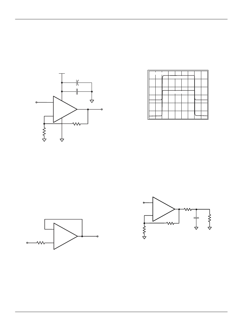
Overdrive Recovery
Overdrive of an amplifier occurs when the output
and/or input ranges are exceeded. The recovery time
varies based on whether the input or output is over-
driven and by how much the ranges are exceeded.
The FAN4272 will typically recover in less than 50ns
from an overdrive condition. Figure 3 shows the
FAN4272 in an overdriven condition.
Figure 3: Overdrive Recovery
Driving Capacitive Loads
The
Frequency Response vs. C
L
plot, illustrates the
response of the FAN4272. A small series resistance (R
s
)
will improve stability and settling performance. R
s
values in the
Frequency Response vs. C
L
plot were
chosen to achieve maximum bandwidth with less than
2dB of peaking. For maximum flatness, use a larger
R
s
. As the plot indicates, the FAN4272 can easily drive
a 50pF capacitive load without a series resistance.
Figure 4: Typical Topology for driving
a capacitive load
Driving a capacitive load introduces phase-lag into
the output signal, which reduces phase margin in the
amplifier. The unity gain follower is the most sensitive
configuration. In a unity gain follower configuration,
the FAN4272 requires a 510
series resistor to drive a
100pF load.
I
Time (10
μ
s/div)
Output
Input
G = 5
-
V
o
KM4270
V
in
+
-
R
f
R
g
R
s
C
L
R
L
DATA SHEET
FAN4272
6
Preliminary September 2001
+
KM4270
-
R
f
0.01
μ
F
6.8
μ
F
+
Out
In
R
g
相关PDF资料 |
PDF描述 |
|---|---|
| FAN4272MX | Voltage-Feedback Operational Amplifier |
| FAN5201MSA | Battery Management |
| FAN5235MTC | Analog IC |
| FAN5235QSC | Analog IC |
| FAN5242QSC | |
相关代理商/技术参数 |
参数描述 |
|---|---|
| FAN4272MX | 制造商:未知厂家 制造商全称:未知厂家 功能描述:Voltage-Feedback Operational Amplifier |
| FAN4274 | 制造商:FAIRCHILD 制造商全称:Fairchild Semiconductor 功能描述:Single and Dual, Ultra-Low Cost, Rail-to-Rail I/O, CMOS Amplifier |
| FAN4274_12 | 制造商:FAIRCHILD 制造商全称:Fairchild Semiconductor 功能描述:Single and Dual, Ultra-Low Cost, Rail-to-Rail I/O, CMOS Amplifier |
| FAN4274IMU8 | 制造商:Rochester Electronics LLC 功能描述:- Bulk |
| FAN4274IMU8X | 功能描述:运算放大器 - 运放 Ang fg Dual Ultra-Lo R-Rail I/O CMOS AmpB RoHS:否 制造商:STMicroelectronics 通道数量:4 共模抑制比(最小值):63 dB 输入补偿电压:1 mV 输入偏流(最大值):10 pA 工作电源电压:2.7 V to 5.5 V 安装风格:SMD/SMT 封装 / 箱体:QFN-16 转换速度:0.89 V/us 关闭:No 输出电流:55 mA 最大工作温度:+ 125 C 封装:Reel |
发布紧急采购,3分钟左右您将得到回复。