- 您现在的位置:买卖IC网 > PDF目录64885 > FAN4822IS (FAIRCHILD SEMICONDUCTOR CORP) 0.5 A POWER FACTOR CONTROLLER, PDSO16 PDF资料下载
参数资料
| 型号: | FAN4822IS |
| 厂商: | FAIRCHILD SEMICONDUCTOR CORP |
| 元件分类: | 稳压器 |
| 英文描述: | 0.5 A POWER FACTOR CONTROLLER, PDSO16 |
| 封装: | PLASTIC, SOIC-16 |
| 文件页数: | 7/10页 |
| 文件大小: | 213K |
| 代理商: | FAN4822IS |
FAN4822
PRODUCT SPECIFICATION
6
REV. 1.0.0 7/26/01
Functional Description
Switching losses of wide input voltage range PFC boost con-
verters increase dramatically as power levels increase above
200 watts. The use of zero-voltage switching (ZVS) tech-
niques improves the efciency of high power PFCs by sig-
nicantly reducing the turn-on losses of the boost MOSFET.
ZVS is accomplished by using a second, smaller MOSFET,
together with a storage element (inductor) to convert the
turn-on losses of the boost MOSFET into useful output
power.
The basic function of the FAN4822 is to provide a power
factor corrected, regulated DC bus voltage using continuous,
average current-mode control. Like Micro Linear’s family of
PFC/PWM controllers, the FAN4822 employs leading-edge
pulse width modulation to reduce system noise and permit
frequency synchronization to a trailing edge PWM stage for
the highest possible DC bus voltage bandwidth. For minimi-
zation of switching losses, circuitry has been incorporated to
control the switching of the ZVS FET.
Theory of Operation
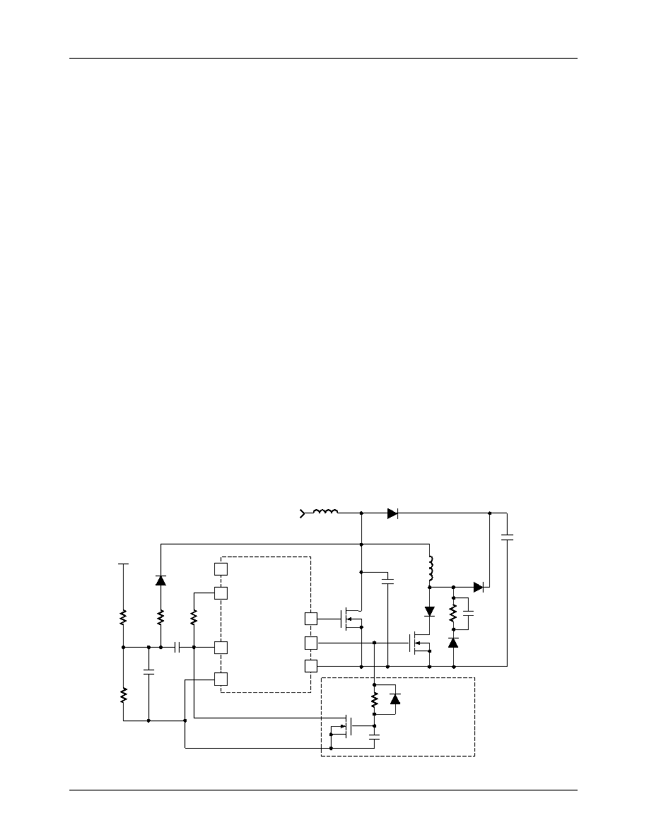
Figure 1 shows a simplied schematic of the output and con-
trol sections of a high power PFC circuit. Figure 2 shows the
relationship of various waveforms in the circuit. Q1 func-
tions as the main switching FET and Q2 provides the ZVS
action. During each cycle, Q2 turns on before Q1, diverting
the current in L1 away from D1 into L2. The current in L2
increases linearly until at t2 it equals the current through L1.
When these currents are equal, L1 ceases discharging current
and is now charged through L2 and Q2. At time t2, the drain
voltage of Q1 begins to fall. The shape of the voltage wave-
form is sinusoidal due to the interaction of L2 and the com-
bined parasitic capacitance of D1 and Q1 (or optional ZVS
capacitor CZVS). At t3, the voltage across Q1 is sufciently
low that the controller turns Q2 off and Q1 on. Q1 then
behaves as an ordinary PFC switch, storing energy in the
boost inductor L1. The energy stored in L2 is completely dis-
charged into the boost capacitor via D2 during the Q1 off-
time and the value of L2 must be selected for discontinuous-
mode operation.
Component Selection
Q1 Turn-Off
Because the FAN4822 uses leading edge modulation, the
PFC MOSFET (Q1) is always turned off at the end of each
oscillator ramp cycle. For proper operation, the internal ZVS
ip-op must be reset every cycle during the oscillator dis-
charge time. This is done by automatically resetting the ZVS
comparator a short time after the drain voltage of the main Q
has reached zero (refer to Figure 1 sense circuit). This sense
circuit terminates the ZVS on time by sensing the main Q
drain voltage reaching zero. It is then reset by way of a resis-
tor pull-up to VCC (R6). The advantage of this circuit is that
the ZVS comparator is not reset at the main Q turn off which
occurs at the end of the clock cycle. This avoids the potential
for improper reset of the internal ZVS ip-op.
Another concern is the proper operation of the ZVS compar-
ator during discontinuous mode operation (DCM), which
will occur at the cusps of the rectied AC waveform and at
light loads. Due to the nature of the voltage seen at the drain
of the main boost Q during DCM operation, the ZVS com-
parator can be fooled into forcing the ZVS Q on for the
entire period. By adding a circuit which limits the maximum
on time of the ZVS Q, this problem can be avoided. Q3 in
Figure 1 provides this function.
Figure 1. Simplified PFC/ZVS Schematic.
11
10
9
8
7
12
C3
33pF
C4
330pF
C5
C1
C2
D1
D2
L1
CZVS(OPT)
+
Q1
Q3
Q2
R1
PFC OUT
ZVS OUT
PWR GND
VCC
13 VREF
VREF
ZV SENSE
GND
FAN4822
MAX ZVS
ON TIME LIMIT
L2
R6
22k
R3
22k
R2
R4
51k
R5
220
相关PDF资料 |
PDF描述 |
|---|---|
| FAN5232MTCX_NL | SWITCHING CONTROLLER, 345 kHz SWITCHING FREQ-MAX, PDSO20 |
| FAN5660MX | SWITCHED CAPACITOR CONVERTER, 90 kHz SWITCHING FREQ-MAX, PDSO8 |
| FAN5660M | SWITCHED CAPACITOR CONVERTER, 90 kHz SWITCHING FREQ-MAX, PDSO8 |
| FAR-D5CM-881M50-D1G1 | 824 MHz(Tx)-849 MHz(Tx), 869 MHz(Rx)-894 MHz(Rx), DUPLEXER |
| FAR-D5CM-881M50-D1M4 | 824 MHz(Tx)-849 MHz(Tx), 869 MHz(Rx)-894 MHz(Rx), DUPLEXER |
相关代理商/技术参数 |
参数描述 |
|---|---|
| FAN4852 | 制造商:FAIRCHILD 制造商全称:Fairchild Semiconductor 功能描述:9MHz Low-Power Dual CMOS Amplifier |
| FAN4852IMU8X | 功能描述:功率放大器 9 MHZ Low Power CMOS Amplifier RoHS:否 制造商:TriQuint Semiconductor 封装 / 箱体: 工作电源电压:28 V 电源电流:2.5 A 工作温度范围: 封装: |
| FAN4855 | 制造商:Fairchild Semiconductor Corporation 功能描述: |
| FAN4855MTC | 功能描述:直流/直流开关调节器 Adj 2-Cell Boost RoHS:否 制造商:International Rectifier 最大输入电压:21 V 开关频率:1.5 MHz 输出电压:0.5 V to 0.86 V 输出电流:4 A 输出端数量: 最大工作温度: 安装风格:SMD/SMT 封装 / 箱体:PQFN 4 x 5 |
| FAN4855MTCX | 功能描述:直流/直流开关调节器 Adj 2-Cell Boost RoHS:否 制造商:International Rectifier 最大输入电压:21 V 开关频率:1.5 MHz 输出电压:0.5 V to 0.86 V 输出电流:4 A 输出端数量: 最大工作温度: 安装风格:SMD/SMT 封装 / 箱体:PQFN 4 x 5 |
发布紧急采购,3分钟左右您将得到回复。