- 您现在的位置:买卖IC网 > PDF目录68993 > FAN5601MU13X (FAIRCHILD SEMICONDUCTOR CORP) SWITCHED CAPACITOR REGULATOR, PDSO8 PDF资料下载
参数资料
| 型号: | FAN5601MU13X |
| 厂商: | FAIRCHILD SEMICONDUCTOR CORP |
| 元件分类: | 稳压器 |
| 英文描述: | SWITCHED CAPACITOR REGULATOR, PDSO8 |
| 封装: | MSOP-8 |
| 文件页数: | 4/15页 |
| 文件大小: | 835K |
| 代理商: | FAN5601MU13X |
PRODUCT SPECIFICATION
FAN5601
12
REV. 1.0.3 5/28/04
Applications Information
Proper operation of the FAN5601 requires one ceramic
bucket capacitor in the 0.1F to 1F range; one 10F output
bypass capacitor and one 10F input bypass capacitor. In
order to obtain optimum output ripple and noise perfor-
mance, use of low ESR (<0.05
) ceramic input and output
bypass capacitors is recommended. The X5R and X7R
rated capacitors provide adequate performance over the
-40C to 85C temperature range.
The value of the bucket capacitor is dependent on load cur-
rent requirements. A 1F bucket capacitor will work well in
all applications at all load currents, while a 0.1F capacitor
will support most applications under 100mA of load current.
The choice of bucket capacitor values should be veried in
the actual application at the lowest input voltage and highest
load current. A 30% margin of safety is recommended in
order to account for the tolerance of the bucket capacitor and
the variations in the on-resistance of the internal switches.
One of the key benets of the ScalarPump architecture is
that the dynamically scaled on-resistance of the switches
effectively reduces the peak current in the bucket capacitor
and therefore input and output ripple current is also reduced.
Nevertheless, due to the ESR of the input and output bypass
capacitors, these current spikes generate voltage spikes at the
input and output pins. However, these ESR spikes can be
easily ltered because their frequency lie at up to 12 times
the clock frequency. In applications where conductive and
radiated EMI/RFI interference has to be kept as low as possi-
ble, the user may consider the use of additional input and
output ltering. For example, adding an L-C lter to the
standard output bypass conguration is very effective in
reducing both the output ripple and the voltage spikes.
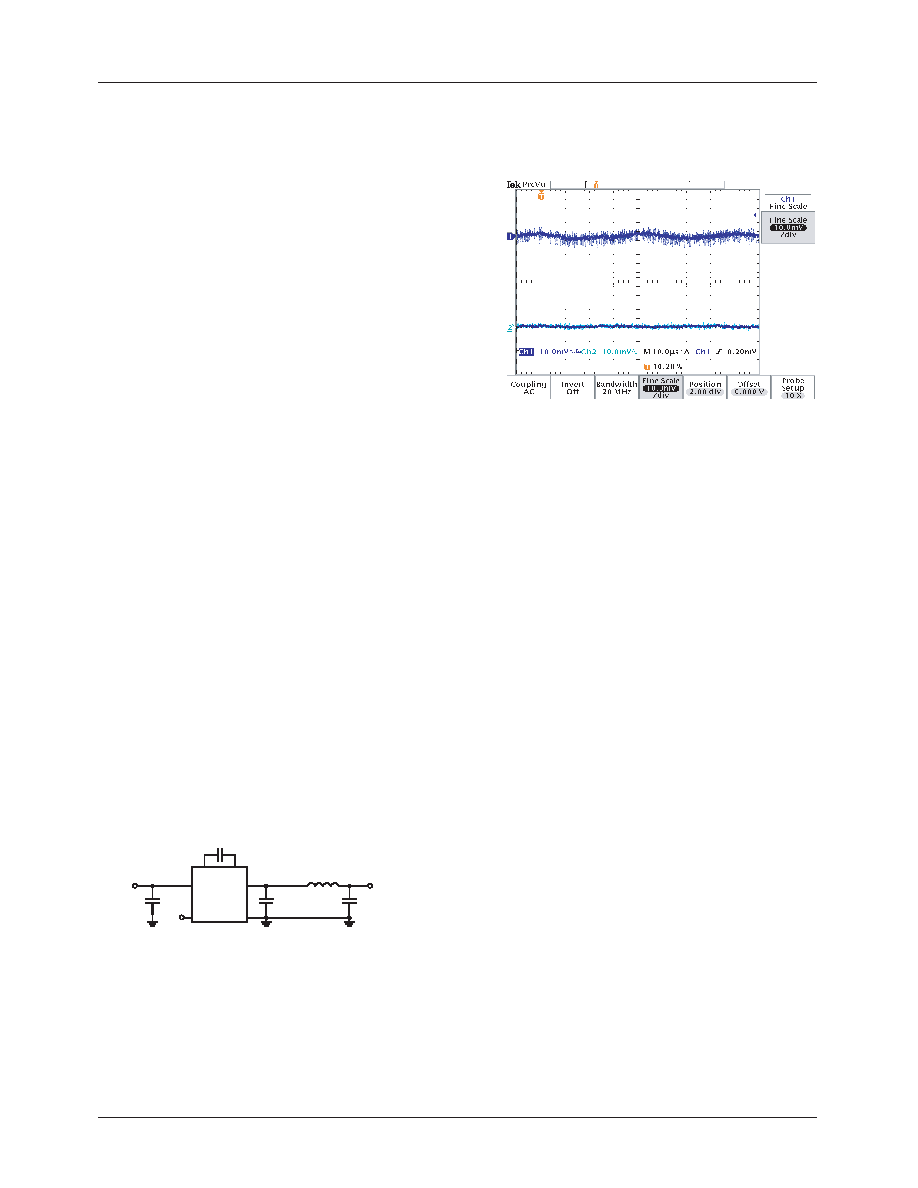
Figure 2 shows an L-C lter using a 100nH chip inductor
and a 1F capacitor. The channel 1 of Figure 3 shows the rip-
ple voltage at the output of the device while Channel 2 shows
the ripple voltage at the output of the lter at VIN = 3.3V,
VOUT = 1.3V and IOUT = 100mA. Similar ltering method
will greatly reduce the current spikes at the input. The user
should be mindful of considering resistive voltage drops in
the inductors connected serially in the input and output
leads.
Figure 3. Effect of L-C Filter on output ripple
While evaluating the FAN5601 (or any other switched
capacitor DC-DC converter) the user should be careful to
keep the power supply source impedance low; use of long
wires causing high lead inductances and resistive losses
should be avoided. A carefully laid out ground plane is
essential because current spikes are generated as the bucket
capacitor is charged and discharged. The input and output
bypass capacitors should be placed as close to the device
pins as possible.
Time (10
s/div)
Output
Ripple
(10mV/di
v)
IOUT = 100mA
VIN = 3.3V
VOUT = 1.3V
Ripple
at
C
F
(1
0mV/d
iv)
Figure 2. Optional L-C Filter
INPUT 2.2V to 5.5V
CB = 1
F
VIN
VOUT
ENABLE
FAN5601
GND
COUT = 10
F
C+
C–
CF = 1
F
LF = 100nH Output 1.0V to 1.8V
CIN = 10
F
相关PDF资料 |
PDF描述 |
|---|---|
| FAN6300DY | SWITCHING CONTROLLER, PDIP8 |
| FAN6300HNY | SWITCHING CONTROLLER, PDIP8 |
| FAN6300ANY | SWITCHING CONTROLLER, PDIP8 |
| FAN6754BMRMY | SWITCHING CONTROLLER, 69 kHz SWITCHING FREQ-MAX, PDSO8 |
| FAN6754BMLMY | SWITCHING CONTROLLER, 69 kHz SWITCHING FREQ-MAX, PDSO8 |
相关代理商/技术参数 |
参数描述 |
|---|---|
| FAN5602 | 制造商:FAIRCHILD 制造商全称:Fairchild Semiconductor 功能描述:Universal (Step-Up/Step-Down) Charge Pump Regulated DC/DC Converter |
| FAN5602_07 | 制造商:FAIRCHILD 制造商全称:Fairchild Semiconductor 功能描述:Universal (Step-Up/Step-Down) Charge Pump Regulated DC/DC Converter |
| FAN5602_0705 | 制造商:FAIRCHILD 制造商全称:Fairchild Semiconductor 功能描述:Universal (Step-Up/Step-Down) Charge Pump Regulated DC/DC Converter |
| FAN5602_09 | 制造商:FAIRCHILD 制造商全称:Fairchild Semiconductor 功能描述:Universal (Step-Up/Step-Down) Charge Pump Regulated DC/DC Converter |
| FAN5602MP33X | 功能描述:电荷泵 Reg Charge Pump DC/DC RoHS:否 制造商:Maxim Integrated 功能:Inverting, Step Up 输出电压:- 1.5 V to - 5.5 V, 3 V to 11 V 输出电流:100 mA 电源电流:1 mA 最大工作温度:+ 70 C 封装 / 箱体:SOIC-8 Narrow 封装:Tube |
发布紧急采购,3分钟左右您将得到回复。