- 您现在的位置:买卖IC网 > PDF目录19197 > FCD7N60TM (Fairchild Semiconductor)MOSFET N-CH 600V 7A DPAK PDF资料下载
参数资料
| 型号: | FCD7N60TM |
| 厂商: | Fairchild Semiconductor |
| 文件页数: | 2/8页 |
| 文件大小: | 0K |
| 描述: | MOSFET N-CH 600V 7A DPAK |
| 产品培训模块: | High Voltage Switches for Power Processing |
| 产品目录绘图: | DPAK, TO-252(AA) |
| 标准包装: | 1 |
| 系列: | SuperFET™ |
| FET 型: | MOSFET N 通道,金属氧化物 |
| FET 特点: | 标准 |
| 漏极至源极电压(Vdss): | 600V |
| 电流 - 连续漏极(Id) @ 25° C: | 7A |
| 开态Rds(最大)@ Id, Vgs @ 25° C: | 600 毫欧 @ 3.5A,10V |
| Id 时的 Vgs(th)(最大): | 5V @ 250µA |
| 闸电荷(Qg) @ Vgs: | 30nC @ 10V |
| 输入电容 (Ciss) @ Vds: | 920pF @ 25V |
| 功率 - 最大: | 83W |
| 安装类型: | 表面贴装 |
| 封装/外壳: | TO-252-3,DPak(2 引线+接片),SC-63 |
| 供应商设备封装: | D-Pak |
| 包装: | 标准包装 |
| 产品目录页面: | 1606 (CN2011-ZH PDF) |
| 其它名称: | FCD7N60TMDKR |
�� �
�
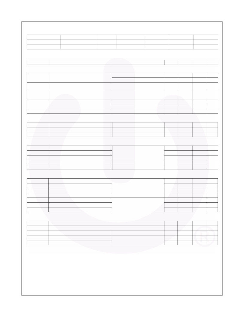
�Package� Marking� and� Ordering� Information�
�Part� Number�
�FCD7N60TM�
�FCD7N60TM_WS�
�Top� Mark�
�FCD7N60�
�FCD7N60�
�Package�
�D-PAK�
�D-PAK�
�Packing� Method�
�Tape� and� Reel�
�Tape� and� Reel�
�Reel� Size�
�330� mm�
�330� mm�
�Tape� Width�
�16� mm�
�16� mm�
�Quantity�
�2500� units�
�2500� units�
�Electrical� Characteristics� T� C� =� 25� o� C� unless� otherwise� noted.�
�Symbol�
�Parameter�
�Test� Conditions�
�Min.�
�Typ.�
�Max.�
�Unit�
�Off� Characteristics�
�BV� DSS�
�Δ� BV� DSS�
�/� Δ� T� J�
�BV� DS�
�I� DSS�
�I� GSS�
�Drain� to� Source� Breakdown� Voltage�
�Breakdown� Voltage� Temperature�
�Coefficient�
�Drain� to� Source� Avalanche� Breakdown�
�Voltage�
�Zero� Gate� Voltage� Drain� Current�
�Gate� to� Body� Leakage� Current�
�V� GS� =� 0� V,� I� D� =� 250� μ� A,� T� C� =� 25� o� C�
�V� GS� =� 0� V,� I� D� =� 250� μ� A,� T� C� =� 150� o� C�
�I� D� =� 250� μ� A,� Referenced� to� 25� o� C�
�V� GS� =� 0� V,� I� D� =� 7.0� A�
�V� DS� =� 600� V,� V� GS� =� 0� V�
�V� DS� =� 480� V,� T� C� =� 125� o� C�
�V� GS� =� ±30� V,� V� DS� =� 0� V�
�600�
�-�
�-�
�-�
�-�
�-�
�-�
�-�
�650�
�0.6�
�700�
�-�
�-�
�-�
�-�
�-�
�-�
�-�
�1�
�10�
�±100�
�V�
�V�
�V/� o� C�
�V�
�μ� A�
�nA�
�On� Characteristics�
�V� GS(th)�
�R� DS(on)�
�g� FS�
�Gate� Threshold� Voltage�
�Static� Drain� to� Source� On� Resistance�
�Forward� Transconductance�
�V� GS� =� V� DS� ,� I� D� =� 250� μ� A�
�V� GS� =� 10� V,� I� D� =� 3.5� A�
�V� DS� =� 40� V,� I� D� =� 3.5� A�
�3.0�
�-�
�-�
�-�
�0.53�
�6�
�5.0�
�0.6�
�-�
�V�
�Ω�
�S�
�Dynamic� Characteristics�
�C� iss�
�C� oss�
�C� rss�
�C� oss�
�C� oss(eff.)�
�Input� Capacitance�
�Output� Capacitance�
�Reverse� Transfer� Capacitance�
�Output� Capacitance�
�Effective� Output� Capacitance�
�V� DS� =� 25� V,� V� GS� =� 0� V,�
�f� =� 1� MHz�
�V� DS� =� 480� V,� V� GS� =� 0� V,� f� =� 1� MHz�
�V� DS� =� 0� V� to� 400� V,� V� GS� =� 0� V�
�-�
�-�
�-�
�-�
�-�
�710�
�380�
�34�
�22�
�60�
�920�
�500�
�-�
�29�
�-�
�pF�
�pF�
�pF�
�pF�
�pF�
�Switching� Characteristics�
�t� d(on)�
�t� r�
�t� d(off)�
�t� f�
�Turn-On� Delay� Time�
�Turn-On� Rise� Time�
�Turn-Off� Delay� Time�
�Turn-Off� Fall� Time�
�V� DD� =� 300� V,� I� D� =� 7.0� A,�
�V� GS� =� 10� V� ,� R� G� =� 25� Ω�
�(Note� 4)�
�-�
�-�
�-�
�-�
�35�
�55�
�75�
�32�
�80�
�120�
�160�
�75�
�ns�
�ns�
�ns�
�ns�
�Q� g(tot)�
�Q� gs�
�Q� gd�
�Total� Gate� Charge� at� 10V�
�Gate� to� Source� Gate� Charge�
�Gate� to� Drain� “Miller”� Charge�
�V� DS� =� 480� V,� I� D� =� 7.0� A,�
�V� GS� =� 10� V�
�(Note� 4)�
�-�
�-�
�-�
�23�
�4.2�
�11.5�
�30�
�5.5�
�-�
�nC�
�nC�
�nC�
�Drain-Source� Diode� Characteristics�
�I� S�
�I� SM�
�Maximum� Continuous� Drain� to� Source� Diode� Forward� Current�
�Maximum� Pulsed� Drain� to� Source� Diode� Forward� Current�
�-�
�-�
�-�
�-�
�7�
�21�
�A�
�A�
�V� SD�
�t� rr�
�Q� rr�
�Drain� to� Source� Diode� Forward� Voltage�
�Reverse� Recovery� Time�
�Reverse� Recovery� Charge�
�V� GS� =� 0� V,� I� SD� =� 7.0� A�
�V� GS� =� 0� V,� I� SD� =� 7.0� A,�
�dI� F� /dt� =� 100� A/� μ� s�
�-�
�-�
�-�
�-�
�360�
�4.5�
�1.4�
�-�
�-�
�V�
�ns�
�μ� C�
�Notes:�
�1.� Repetitive� rating:� pulse-width� limited� by� maximum� junction� temperature.�
�2.� I� AS� =� 3.5� A,� V� DD� =� 50� V,� R� G� =� 25� Ω� ,� starting� T� J� =� 25� °� C.�
�3.� I� SD� ≤� 7� A,� di/dt� ≤� 200� A/� μ� s,� V� DD� ≤� BV� DSS� ,� starting� T� J� =� 25� °� C.�
�4.� Essentially� independent� of� operating� temperature� typical� characteristics.�
�?2008� Fairchild� Semiconductor� Corporation�
�FCD7N60� Rev.� C1�
�2�
�www.fairchildsemi.com�
�相关PDF资料 |
PDF描述 |
|---|---|
| PGR-5330-22-00 | GRND RES RELAY PROFIBUS DC SUP |
| PGR-6210-02 | GE RETRO RS-232 DEVICENET CIM |
| PGR-6210-01 | GE RETRO RS-232 RS-485 CIM |
| 210-3MSF | SWITCH RAISED ACTUATOR 3 SEC |
| 210-3LPSF | SWITCH SPST 3 SEC LOW PROFILE |
相关代理商/技术参数 |
参数描述 |
|---|---|
| FCD7N60TM_WS | 功能描述:MOSFET Trans N-Ch 600V 7A 3-Pin 2+Tab RoHS:否 制造商:STMicroelectronics 晶体管极性:N-Channel 汲极/源极击穿电压:650 V 闸/源击穿电压:25 V 漏极连续电流:130 A 电阻汲极/源极 RDS(导通):0.014 Ohms 配置:Single 最大工作温度: 安装风格:Through Hole 封装 / 箱体:Max247 封装:Tube |
| FCD820 | 制造商:FAIRCHILD 制造商全称:Fairchild Semiconductor 功能描述:OPTICALLY-COUPLED ISOLATOR |
| FCD820C | 制造商:FAIRCHILD 制造商全称:Fairchild Semiconductor 功能描述:OPTICALLY-COUPLED ISOLATOR |
| FCD860 | 制造商:未知厂家 制造商全称:未知厂家 功能描述:Optoelectronic |
| FCD860C | 制造商:未知厂家 制造商全称:未知厂家 功能描述:Optoelectronic |
发布紧急采购,3分钟左右您将得到回复。