- 您现在的位置:买卖IC网 > PDF目录10718 > FIN1018MX (Fairchild Semiconductor)RECEIVER 3.3V LVDS HS 8SOIC PDF资料下载
参数资料
| 型号: | FIN1018MX |
| 厂商: | Fairchild Semiconductor |
| 文件页数: | 2/8页 |
| 文件大小: | 0K |
| 描述: | RECEIVER 3.3V LVDS HS 8SOIC |
| 产品变化通告: | Mold Compound Change 12/Sept/2008 |
| 标准包装: | 1 |
| 类型: | 接收器 |
| 驱动器/接收器数: | 0/1 |
| 规程: | LVDS |
| 电源电压: | 3 V ~ 3.6 V |
| 安装类型: | 表面贴装 |
| 封装/外壳: | 8-SOIC(0.154",3.90mm 宽) |
| 供应商设备封装: | 8-SOICN |
| 包装: | 标准包装 |
| 其它名称: | FIN1018MXDKR |
www.fairchildsemi.com
2
FIN1018
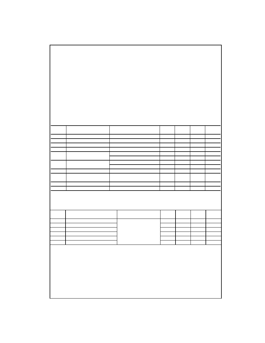
Absolute Maximum Ratings(Note 1)
Recommended Operating
Conditions
Note 1: The “Absolute Maximum Ratings”: are those values beyond which
damage to the device may occur. The databook specifications should be
met, without exception, to ensure that the system design is reliable over its
power supply, temperature and output/input loading variables. Fairchild
does not recommend operation of circuits outside databook specification.
DC Electrical Characteristics
Over supply voltage and operating temperature ranges, unless otherwise specified
Note 2: All typical values are at TA = 25°C and with VCC = 3.3V.
AC Electrical Characteristics
Over supply voltage and operating temperature ranges, unless otherwise specified
Note 3: All typical values are at TA = 25°C and with VCC = 3.3V.
Note 4: tSK(PP) is the magnitude of the difference in propagation delay times between any specified terminals of two devices switching in the same direction
(either LOW-to-HIGH or HIGH-to-LOW) when both devices operate with the same supply voltage, same temperature, and have identical test circuits.
Supply Voltage (VCC)
0.5V to +4.6V
DC Input Voltage (RIN+, RIN)
0.5V to +4.7V
DC Output Voltage (DOUT)
0.5V to +6V
DC Output Current (IO)16 mA
Storage Temperature Range (TSTG)
65°C to +150°C
Max Junction Temperature (TJ)150°C
Lead Temperature (TL)
(Soldering, 10 seconds)
260
°C
ESD (Human Body Model)
≥ 6500V
ESD (Bus Pins RIN/RIN+ to GND)
≥ 9500V
ESD (Machine Model)
≥ 300V
Supply Voltage (VCC)
3.0V to 3.6V
Input Voltage (VIN)
0 to VCC
Magnitude of Differential Voltage
(|VID|)
100mV to VCC
Common-mode Input Voltage (VIC)
0.05V to 2.35V
Operating Temperature (TA)
40°C to +85°C
Symbol
Parameter
Test Conditions
Min
Typ
Max
Units
(Note 2)
VTH
Differential Input Threshold HIGH
See Figure 1 and Table 1
100
mV
VTL
Differential Input Threshold LOW
See Figure 1 and Table 1
100
mV
IIN
Input Current
VIN = 0V or VCC
±20
A
II(OFF)
Power-OFF Input Current
VCC = 0V, VIN = 0V or 3.6V
±20
A
VOH
Output HIGH Voltage
IOH = 100 AVCC 0.2
V
IOH = 8 mA
2.4
V
VOL
Output LOW Voltage
IOH = 100 A0.2
V
IOL = 8 mA
0.5
V
VIK
Input Clamp Voltage
IIK = 18 mA
1.5
V
ICC
Power Supply Current
Inputs Open, (RIN+ = 1V and RIN = 1.4V),
7mA
or (RIN+ = 1.4V and RIN = 1V)
CIN
Input Capacitance
4pF
COUT
Output Capacitance
6pF
Symbol
Parameter
Test Conditions
Min
Typ
Max
Units
(Note 3)
tPLH
Propagation Delay LOW-to-HIGH
0.9
2.5
ns
tPHL
Propagation Delay HIGH-to-LOW
0.9
2.5
ns
tTLH
Output Rise Time (20% to 80%)
|VID| = 400 mV, CL = 10 pF
0.5
ns
tTHL
Output Fall Time (80% to 20%)
See Figure 1 and Figure 2
0.5
ns
tSK(P)
Pulse Skew |tPLH - tPHL|
0.4
ns
tSK(PP)
Part-to-Part Skew (Note 4)
1.0
ns
相关PDF资料 |
PDF描述 |
|---|---|
| VE-25N-MY-B1 | CONVERTER MOD DC/DC 18.5V 50W |
| VE-25L-MY-B1 | CONVERTER MOD DC/DC 28V 50W |
| VE-24T-MY-B1 | CONVERTER MOD DC/DC 6.5V 50W |
| VE-24R-MY-B1 | CONVERTER MOD DC/DC 7.5V 50W |
| USB1T20MTCX | TRANSCEIVER USB 14-TSSOP |
相关代理商/技术参数 |
参数描述 |
|---|---|
| FIN1019 | 制造商:FAIRCHILD 制造商全称:Fairchild Semiconductor 功能描述:3.3V LVDS High Speed Differential Driver/Receiver |
| FIN1019M | 功能描述:缓冲器和线路驱动器 3.3V Driver/Receiver Hi Speed Diff LVDS RoHS:否 制造商:Micrel 输入线路数量:1 输出线路数量:2 极性:Non-Inverting 电源电压-最大:+/- 5.5 V 电源电压-最小:+/- 2.37 V 最大工作温度:+ 85 C 安装风格:SMD/SMT 封装 / 箱体:MSOP-8 封装:Reel |
| FIN1019M_Q | 功能描述:总线收发器 3.3V Driver/Receiver Hi Speed Diff LVDS RoHS:否 制造商:Fairchild Semiconductor 逻辑类型:CMOS 逻辑系列:74VCX 每芯片的通道数量:16 输入电平:CMOS 输出电平:CMOS 输出类型:3-State 高电平输出电流:- 24 mA 低电平输出电流:24 mA 传播延迟时间:6.2 ns 电源电压-最大:2.7 V, 3.6 V 电源电压-最小:1.65 V, 2.3 V 最大工作温度:+ 85 C 封装 / 箱体:TSSOP-48 封装:Reel |
| FIN1019MMTC | 制造商:FAIRCHILD 制造商全称:Fairchild Semiconductor 功能描述:LINE TRANSCEIVER|1 DRIVER|1 RCVR|TSSOP|14PIN|PLASTIC |
| FIN1019MMTCX | 制造商:FAIRCHILD 制造商全称:Fairchild Semiconductor 功能描述:LINE TRANSCEIVER|1 DRIVER|1 RCVR|TSSOP|14PIN|PLASTIC |
发布紧急采购,3分钟左右您将得到回复。