- 您现在的位置:买卖IC网 > PDF目录1920 > FIN1104MTCX (Fairchild Semiconductor)IC REPEATER 4 PORT LVDS 24-TSSOP PDF资料下载
参数资料
| 型号: | FIN1104MTCX |
| 厂商: | Fairchild Semiconductor |
| 文件页数: | 3/6页 |
| 文件大小: | 0K |
| 描述: | IC REPEATER 4 PORT LVDS 24-TSSOP |
| 标准包装: | 1 |
| 类型: | 转发器 |
| Tx/Rx类型: | LVDS |
| 延迟时间: | 1.75ns |
| 电容 - 输入: | 2.6pF |
| 电源电压: | 3 V ~ 3.6 V |
| 电流 - 电源: | 41mA |
| 安装类型: | 表面贴装 |
| 封装/外壳: | 24-TSSOP(0.173",4.40mm 宽) |
| 供应商设备封装: | 24-TSSOP |
| 包装: | 标准包装 |
| 其它名称: | FIN1104MTCXDKR |
3
www.fairchildsemi.com
FI
N1
104
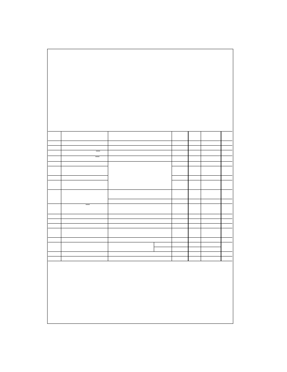
Absolute Maximum Ratings(Note 1)
Recommended Operating
Conditions
Note 1: The “Absolute Maximum Ratings”: are those values beyond which
damage to the device may occur. The databook specifications should be
met, without exception, to ensure that the system design is reliable over its
power supply, temperature and output/input loading variables. Fairchild
does not recommend operation of circuits outside databook specification.
DC Electrical Characteristics
Note 2: All typical values are at TA = 25°C and with VCC = 3.3V.
Supply Voltage (VCC)
0.5V to +4.6V
LVDS DC Input Voltage (VIN)
0.5V to +4.6V
LVDS DC Output Voltage (VOUT)
0.5V to +4.6V
Driver Short Circuit Current (IOSD)
Continuous 10 mA
Storage Temperature Range (TSTG)
65°C to +150°C
Max Junction Temperature (TJ)150°C
Lead Temperature (TL)
(Soldering, 10 seconds)
260
°C
ESD (Human Body Model)
7500V
ESD (Machine Model)
400V
Supply Voltage (VCC)
3.0V to 3.6V
Magnitude of Differential
Voltage (|VID|)
100 mV to VCC
Common Mode Voltage
Range (VIC)(0V + |VID|/2) to (VCC |VID|/2)
Operating Temperature (TA)
40°C to +85°C
Symbol
Parameter
Test Conditions
Min
Typ
Max
Units
(Note 2)
VTH
Differential Input Threshold HIGH
See Figure 1; VIC = +0.05V, +1.2V, or VCC 0.05V
100
mV
VTL
Differential Input Threshold LOW
See Figure 1; VIC = +0.05V, +1.2V, or VCC 0.05V
100
mV
VIH
Input HIGH Voltage (EN or EN)2.0
VCC
V
VIL
Input LOW Voltage (EN or EN)GND
0.8
V
VOD
Output Differential Voltage
250
330
450
mV
V
OD
VOD Magnitude Change from
25
mV
Differential LOW-to-HIGH
RL = 100 , Driver Enabled,
VOS
Offset Voltage
See Figure 2
1.125
1.23
1.375
V
OS
Offset Magnitude Change from
25
mV
Differential LOW-to-HIGH
IOS
Short Circuit Output Current
DOUT+ = 0V and DOUT = 0V,
3.4
6mA
Driver Enabled
VOD = 0V, Driver Enabled
±3.4
±6mA
IIN
Input Current (EN, EN, DINx+, DINx)VIN = 0V to VCC, Other Input = VCC or 0V
±20
A
(for Differential Inputs)
IOFF
Power Off Input or Output Current
VCC = 0V, VIN or VOUT = 0V to 3.6V
±20
A
ICCZ
Disabled Power Supply Current
Drivers Disabled
5.4
11
mA
ICC
Power Supply Current
Drivers Enabled, Any Valid Input Condition
30.4
41
mA
IOZ
Disabled Output Leakage Current
Driver Disabled, DOUT+ = 0V to 3.6V or
±20
A
DOUT = 0V to3.6V
VIC
Common Mode Voltage Range
|VID| = 100 mV to VCC
0V
+ |V
ID|/2
VCC (|VID|/2)
V
CIN
Input Capacitance
Enable Input
2.6
pF
LVDS Input
2.1
COUT
Output Capacitance
2.8
pF
VBB
Output Reference Voltage
VCC = 3.3V, IBB = 0 to 275 A
1.125
1.2
1.375
V
相关PDF资料 |
PDF描述 |
|---|---|
| FIN1108MTDX | IC REPEATER 8PORT LVDS 48-TSSOP |
| FIN1218MTDX | IC SERIALIZER/DESERIAL 48-TSSOP |
| FIN1531MTCX | IC DRIVER 5V LVDS 4BIT 16TSSOP |
| FIN1532MX_NF40 | IC RCVR HS DIFF 5V LVDS 16-SOIC |
| FIN210ACMLX | IC SER/DES 10BIT 32-MLP |
相关代理商/技术参数 |
参数描述 |
|---|---|
| FIN1104MTCX | 制造商:Fairchild Semiconductor Corporation 功能描述:Driver IC |
| FIN1108 | 制造商:FAIRCHILD 制造商全称:Fairchild Semiconductor 功能描述:LVDS 8 Port High Speed Repeater |
| FIN1108_10 | 制造商:FAIRCHILD 制造商全称:Fairchild Semiconductor 功能描述:LVDS 8-Port, High-Speed Repeater |
| FIN1108MTD | 功能描述:缓冲器和线路驱动器 8 Port Repeater LVDS Hi Speed RoHS:否 制造商:Micrel 输入线路数量:1 输出线路数量:2 极性:Non-Inverting 电源电压-最大:+/- 5.5 V 电源电压-最小:+/- 2.37 V 最大工作温度:+ 85 C 安装风格:SMD/SMT 封装 / 箱体:MSOP-8 封装:Reel |
| FIN1108MTD | 制造商:Fairchild Semiconductor Corporation 功能描述:IC LVDS REPEATER 800MBPS 3.3V TSSOP48 |
发布紧急采购,3分钟左右您将得到回复。