- 您现在的位置:买卖IC网 > PDF目录68995 > FMS2704T1C (FAIRCHILD SEMICONDUCTOR CORP) SPECIALTY ANALOG CIRCUIT, PDSO24 PDF资料下载
参数资料
| 型号: | FMS2704T1C |
| 厂商: | FAIRCHILD SEMICONDUCTOR CORP |
| 元件分类: | 模拟信号调理 |
| 英文描述: | SPECIALTY ANALOG CIRCUIT, PDSO24 |
| 封装: | TSSOP-24 |
| 文件页数: | 16/39页 |
| 文件大小: | 173K |
| 代理商: | FMS2704T1C |
第1页第2页第3页第4页第5页第6页第7页第8页第9页第10页第11页第12页第13页第14页第15页当前第16页第17页第18页第19页第20页第21页第22页第23页第24页第25页第26页第27页第28页第29页第30页第31页第32页第33页第34页第35页第36页第37页第38页第39页
FMS2704/FMS2704L
PRODUCT SPECIFICATION
REV. 1.01 12/2/99
23
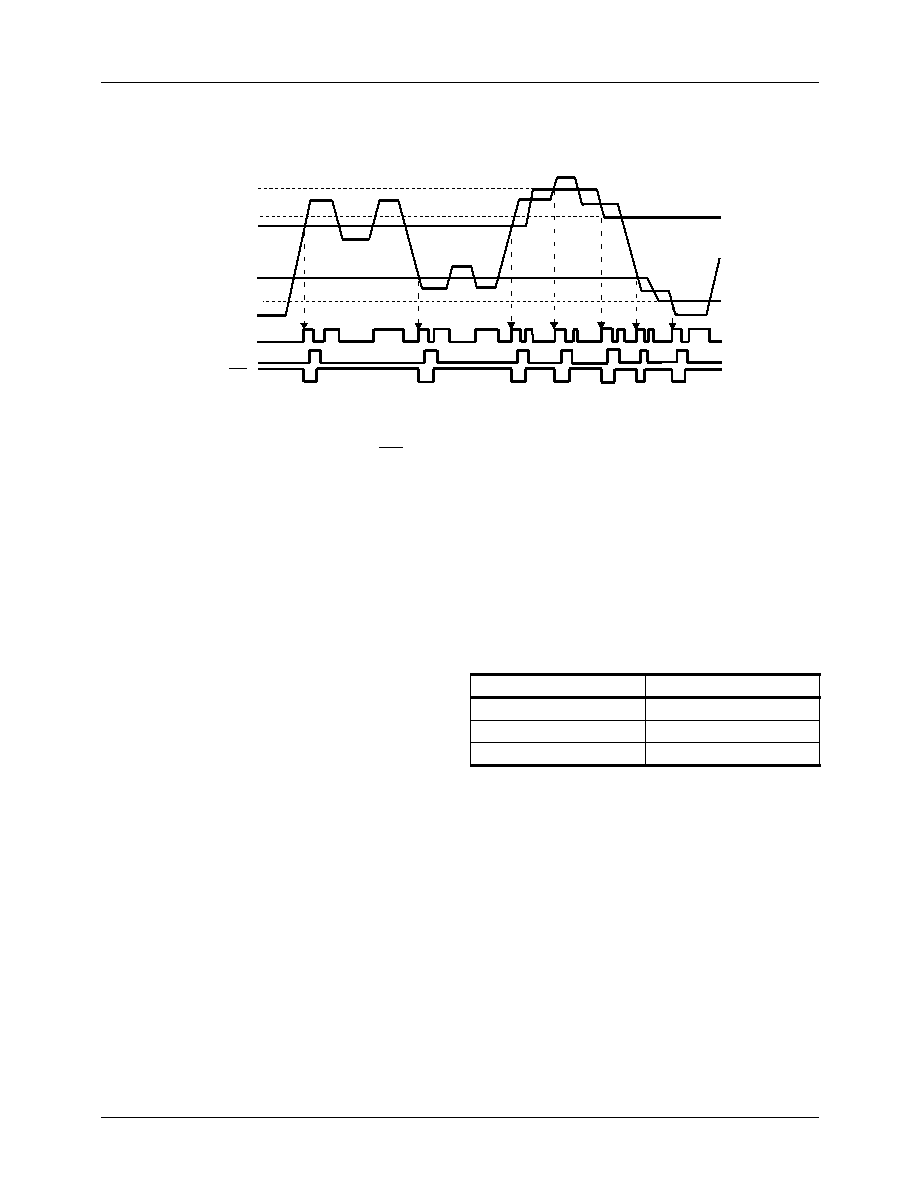
Temperature limits are xed for the rst series of temperature
excursions. Then, for the second series, following the THI1
violation, the THI limit is raised from THI1 to THI2. If THI is
reprogrammed from a value above T to a value below THI,
then an interrupt is generated.
Figure 7. Profile of Temperature Driven Interrupts
INT
T
THI1
THI2
THI3
TLO1
TLO2
RTV/LTV
Read_INT
LTV and RTV bits operate in conjunction with the INT output
and Interrupt Status Register as follows:
1.
When the temperature exceeds a high limit, the corre-
sponding Interrupt Status Register bit, either LTV or
RTV is set.
2.
Reading the Interrupt Status Register clears LTV and
RTV.
3.
Once the high limit has been exceeded, a subsequent
transitions through the high level will not cause an
interrupt, unless:
a) The temperature passes through the low limit.
b) Or, the high temperature limit is changed.
4.
If the high temperature limit is changed from a level
above the temperature to a level below, then the relevant
Interrupt Status Register bit, either LTV or RTV is set.
5.
If the temperature falls below a low limit, the corre-
sponding Interrupt Status Register bit, either LTV or
RTV is set.
6.
Once the low limit has been exceeded, a subsequent
transitions through the low level will not cause an inter-
rupt, unless:
a) The temperature passes through the high limit.
b) Or, the low temperature limit is changed.
If the low temperature limit is changed from a level below the
ambient/remote temperature to a level above, then the LTV/
RTV bit is set.
Serial Interface
FMS2704 register access is via a 2-wire I2C/SMBus compati-
ble interface. Base address is 0x2C + n, where n is an offset
dened by the state of the ADD pin: Z, H, L == 0, 1, 2. (see
Table 3) State Z corresponds to the ADD pin being open
circuit.
Two signals comprise the bus: clock (SCL) and bi-directional
data (SDA). When receiving and transmitting data through the
serial interface, the FMS2704 acts as a slave, responding only
to commands by the I2C/SMBus master.
Data received or transmitted on the SDA line must be stable
for the duration of the positive-going SCL pulse. Data on
SDA may change only when SCL = L. An SDA transition
while SCL = H is interpreted as a start or stop signal.
Table 3. Serial Port Slave Addresses
ADD
Address
Z
2C
H
2D
L
2E
相关PDF资料 |
PDF描述 |
|---|---|
| FMS6501MSA28X_NL | 12-CHANNEL, AUDIO/VIDEO SWITCH, PDSO28 |
| FN3000-810-830 | PLL FREQUENCY SYNTHESIZER, DMA37 |
| FNA41060 | AC MOTOR CONTROLLER, DMA26 |
| FNB41560 | AC MOTOR CONTROLLER, DMA26 |
| FNW500R4 | 1-OUTPUT 504 W DC-DC REG PWR SUPPLY MODULE |
相关代理商/技术参数 |
参数描述 |
|---|---|
| FMS2A | 制造商:ROHM Semiconductor 功能描述:100 mA, 40 V, 2 CHANNEL, PNP, Si, SMALL SIGNAL TRANSISTOR |
| FMS2T148 | 制造商:ROHM Semiconductor 功能描述: |
| FMS3 | 制造商:MITA 功能描述:12M COIL SA 38X16MM TRUNK |
| FMS300 | 制造商:Black Box Corporation 功能描述:CAT6 SHIELDED JACK 90 DEGREE |
| FMS3110 | 制造商:FAIRCHILD 制造商全称:Fairchild Semiconductor 功能描述:Triple Video D/A Converters 3 x 10 bit, 150 Ms/s |
发布紧急采购,3分钟左右您将得到回复。