- 您现在的位置:买卖IC网 > PDF目录67505 > FMS3120KRC (FAIRCHILD SEMICONDUCTOR CORP) TRIPLE, PARALLEL, WORD INPUT LOADING, 10-BIT DAC, PQFP48 PDF资料下载
参数资料
| 型号: | FMS3120KRC |
| 厂商: | FAIRCHILD SEMICONDUCTOR CORP |
| 元件分类: | DAC |
| 英文描述: | TRIPLE, PARALLEL, WORD INPUT LOADING, 10-BIT DAC, PQFP48 |
| 封装: | LQFP-48 |
| 文件页数: | 12/12页 |
| 文件大小: | 143K |
| 代理商: | FMS3120KRC |
PRODUCT SPECIFICATION
FMS3110/3115/3120/3125
REV. 1.03 9/19/00
9
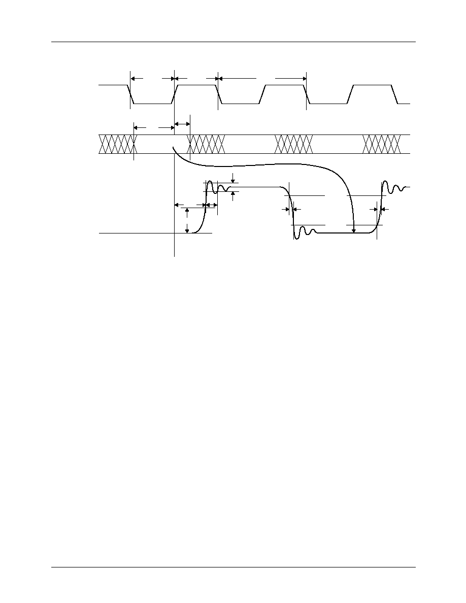
Timing Diagram
CLK
PIXEL DATA
& CONTROLS
OUTPUT
DataN
DataN+1
DataN+2
tPWL
tS
tH
50%
3%/FS
90%
10%
tD
tSET
tF
tR
tPWH
1/fS
Applications Discussion
Figure 5 illustrates a typical FMS3110/3115/3120/3125
interface circuit. In this example, an optional 1.2 Volt band-
gap reference is connected to the VREF output, overriding
the internal voltage reference source.
Grounding
It is important that the FMS3110/3115/3120/3125 power
supply is well-regulated and free of high-frequency noise.
Careful power supply decoupling will ensure the highest
quality video signals at the output of the circuit. The
FMS3110/3115/3120/3125 has separate analog and digital
circuits. To keep digital system noise from the D/A converter,
it is recommended that power supply voltages (VDD) come
from the system analog power source and all ground connec-
tions (GND) be made to the analog ground plane. Power supply
pins should be individually decoupled at the pin.
Printed Circuit Board Layout
Designing with high-performance mixed-signal circuits
demands printed circuits with ground planes. Overall system
performance is strongly inuenced by the board layout.
Capacitive coupling from digital to analog circuits may
result in poor D/A conversion. Consider the following sug-
gestions when doing the layout:
1.
Keep the critical analog traces (VREF, IREF, COMP,
IOS, IOR, IOG) as short as possible and as far as possi-
ble from all digital signals. The FMS3110/3115/3120/
3125 should be located near the board edge, close to the
analog output connectors.
2.
Power plane for the FMS3110/3115/3120/3125 should
be separate from that which supplies the digital cir-
cuitry. A single power plane should be used for all of the
VDD pins. If the power supply for the FMS3110/3115/
3120/3125 is the same as that of the system's digital cir-
cuitry, power to the FMS3110/3115/3120/3125 should
be decoupled with 0.1F and 0.01F capacitors and iso-
lated with a ferrite bead.
3.
The ground plane should be solid, not cross-hatched.
Connections to the ground plane should have very short
leads.
4.
If the digital power supply has a dedicated power plane
layer, it should not be placed under the FMS3110/3115/
3120/3125, the voltage reference, or the analog outputs.
Capacitive coupling of digital power supply noise from
this layer to the FMS3110/3115/3120/3125 and its
related analog circuitry can have an adverse effect on
performance.
5.
CLK should be handled carefully. Jitter and noise on
this clock will degrade performance. Terminate the
clock line carefully to eliminate overshoot and ringing.
Related Products
FMS38XX Triple 8-bit 250 Msps D/A Converters
FMS9884A 3 x 8-bit 200 Ms/s A/D Converter
相关PDF资料 |
PDF描述 |
|---|---|
| FMS3125KRC | TRIPLE, PARALLEL, WORD INPUT LOADING, 10-BIT DAC, PQFP48 |
| FMS3810KRC_NL | PARALLEL, 8 BITS INPUT LOADING, 1400 us SETTLING TIME, 8-BIT DAC, PQFP48 |
| FMS3815KRC_NL | PARALLEL, 8 BITS INPUT LOADING, 8-BIT DAC, PQFP48 |
| FMS3820KRC | PARALLEL, 8 BITS INPUT LOADING, 1700 us SETTLING TIME, 8-BIT DAC, PQFP48 |
| FMS3825KRC | TRIPLE, PARALLEL, 8 BITS INPUT LOADING, 8-BIT DAC, PQFP48 |
相关代理商/技术参数 |
参数描述 |
|---|---|
| FMS3125KRC | 制造商:未知厂家 制造商全称:未知厂家 功能描述:Video DAC without Color Palette |
| FMS3810 | 制造商:FAIRCHILD 制造商全称:Fairchild Semiconductor 功能描述:PCB Layout Considerations for Video Filter / Drivers |
| FMS3810KRC | 功能描述:数模转换器- DAC 100Mhz D/a Converter 8Bit Tripple Video RoHS:否 制造商:Texas Instruments 转换器数量:1 DAC 输出端数量:1 转换速率:2 MSPs 分辨率:16 bit 接口类型:QSPI, SPI, Serial (3-Wire, Microwire) 稳定时间:1 us 最大工作温度:+ 85 C 安装风格:SMD/SMT 封装 / 箱体:SOIC-14 封装:Tube |
| FMS3810KRCT | 功能描述:数模转换器- DAC 100Mhz D/a Converter 8Bit Tripple Video RoHS:否 制造商:Texas Instruments 转换器数量:1 DAC 输出端数量:1 转换速率:2 MSPs 分辨率:16 bit 接口类型:QSPI, SPI, Serial (3-Wire, Microwire) 稳定时间:1 us 最大工作温度:+ 85 C 安装风格:SMD/SMT 封装 / 箱体:SOIC-14 封装:Tube |
| FMS-38141-E | 制造商:GC Electronics 功能描述: |
发布紧急采购,3分钟左右您将得到回复。