参数资料
| 型号: | FMS6141CS |
| 厂商: | Fairchild Semiconductor |
| 文件页数: | 7/11页 |
| 文件大小: | 0K |
| 描述: | IC VIDEO FILTER DRIVER 8-SOIC |
| 产品变化通告: | Mold Compound Change 12/Sept/2008 |
| 标准包装: | 95 |
| 类型: | 视频滤波器 |
| 应用: | DVD,HD,机顶盒,录音机 |
| 安装类型: | 表面贴装 |
| 封装/外壳: | 8-SOIC(0.154",3.90mm 宽) |
| 供应商设备封装: | 8-SOICN |
| 包装: | 管件 |
FMS6141
—
Low-Cost,
Single-Channel
4
th
-Order
Standard
Definition
Video
Filter
Driver
2006 Fairchild Semiconductor Corporation
www.fairchildsemi.com
FMS6141 Rev. 1.0.3
5
Application Information
Input Considerations
The FMS6141 Low-Cost Video Filter provides 6 dB (2X)
gain from input to output. The device provides an
internal diode clamp to support AC-coupled input
signals. In this configuration, a 0.1 F ceramic capacitor
is used to AC couple the input signal. If the input signal
does not go below ground, the clamp is inactive; but if
the input signal goes below ground, the clamp circuitry
sets the bottom of the sync tip (or lowest voltage) to just
below ground. The input level set by the clamp,
combined with the internal DC offset, keeps the output
signal within an acceptable range. This clamp feature
also allows the FMS6141’s input to be directly driven
(DC-coupled) by a ground referenced DAC output.
Figure 4 shows typical DC voltage levels for the input
and output signals when driven by a DC-coupled DAC
output or an AC-coupled and clamped Y, CV signal.
0.28V
0.88V
1.58V
2.28V
0.0 -> 0.02V
0.3 -> 0.32V
0.65 -> 0.67V
1.0 -> 1.02V
Vin
Vout
Figure 4. Typical DC Voltage Levels
Output Considerations
The FMS6141 outputs will be DC offset from the input
by 150 mv therefore VOUT = 2*VIN DC+150 mv. This
offset is required to obtain optimal performance from the
output driver and is held at the minimum value in order
to decrease the standing DC current into the load. Since
the FMS6141 has a 2x (6 dB) gain, the output is typically
connected via a 75 series back-matching resistor
followed by the 75 video cable. Because of the
inherent divide by two of this configuration, the blanking
level at the load of the video signal is always less then
1 V. When AC-coupling the output ensure that the
coupling capacitor of choice will pass the lowest
frequency content in the video signal and that line time
distortion (video tilt) is kept as low as possible.
The selection of the coupling capacitor is a function of
the subsequent circuit input impedance and the leakage
current of the input being driven. In order to obtain the
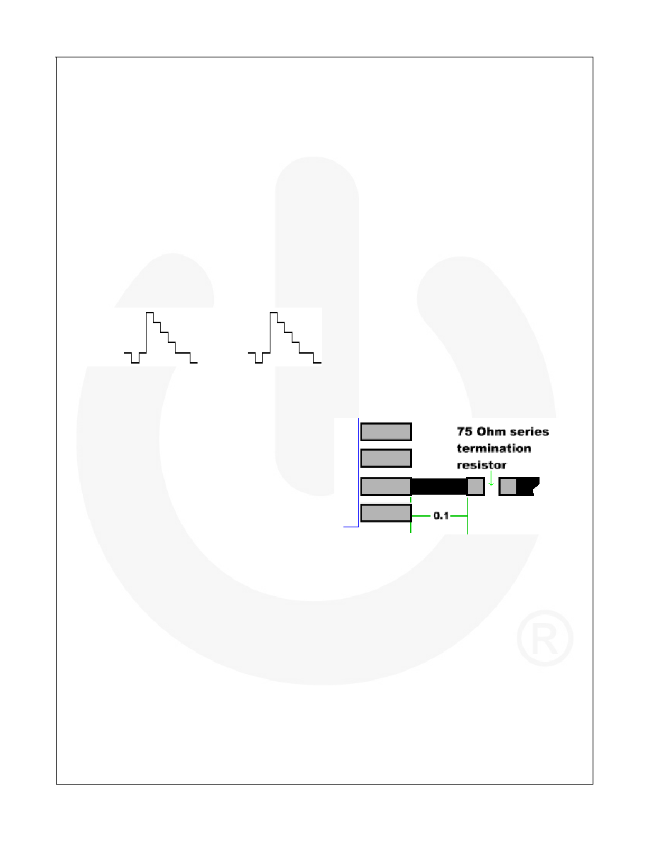
highest quality output video signal the series termination
resistor must be placed as close to the device output pin
as possible. This greatly reduces the parasitic
capacitance and inductance effect on the FMS6141
output driver. Recommend distance from device pin to
place series termination resistor should be no greater
than 0.1 inches.
Figure 5. Distance from Device Pin to Series
Termination Resistor
相关PDF资料 |
PDF描述 |
|---|---|
| FMS6143ACSX | IC DRIVER VIDEO FILTER 1CH 8SOIC |
| FMS6143CS | IC DRIVER VIDEO FILTER 3CH 8SOIC |
| FMS6144AMTC14X | IC DVR VID FILTER SD 4CH 14TSSOP |
| FMS6145MTC14 | IC DRIVER VIDEO FLTR 5CH 14TSSOP |
| FMS6146MTC14 | IC DRIVER VIDEO FLTR 6CH 14TSSOP |
相关代理商/技术参数 |
参数描述 |
|---|---|
| FMS6141CSX | 功能描述:有源滤波器 1-Ch 4th Order Std Video Filter Driver RoHS:否 制造商:Maxim Integrated 通道数量:1 截止频率:150 KHz 电源电压-最大:11 V 电源电压-最小:4.74 V 最大工作温度:+ 85 C 安装风格:Through Hole 封装 / 箱体:PDIP N 封装:Tube |
| FMS6141CSX | 制造商:Fairchild Semiconductor Corporation 功能描述:FILTER DRIVER VIDEO SMD SOIC8 |
| FMS6141S5X | 功能描述:有源滤波器 1-Ch 4th Order Std Video Filter Driver RoHS:否 制造商:Maxim Integrated 通道数量:1 截止频率:150 KHz 电源电压-最大:11 V 电源电压-最小:4.74 V 最大工作温度:+ 85 C 安装风格:Through Hole 封装 / 箱体:PDIP N 封装:Tube |
| FMS6141S5X-CUT TAPE | 制造商:FAIRCHILD 功能描述:FMS Series 6 V 7.7 MHz Low Cost Single Channel Video Filter Driver - SC-70-5 |
| FMS6143 | 制造商:FAIRCHILD 制造商全称:Fairchild Semiconductor 功能描述:PCB Layout Considerations for Video Filter / Drivers |
发布紧急采购,3分钟左右您将得到回复。