- 您现在的位置:买卖IC网 > PDF目录67505 > FMS9874AKGC140 (FAIRCHILD SEMICONDUCTOR CORP) 3-CH 8-BIT PROPRIETARY METHOD ADC, PARALLEL ACCESS, PQFP100 PDF资料下载
参数资料
| 型号: | FMS9874AKGC140 |
| 厂商: | FAIRCHILD SEMICONDUCTOR CORP |
| 元件分类: | ADC |
| 英文描述: | 3-CH 8-BIT PROPRIETARY METHOD ADC, PARALLEL ACCESS, PQFP100 |
| 封装: | MQFP-100 |
| 文件页数: | 26/26页 |
| 文件大小: | 454K |
| 代理商: | FMS9874AKGC140 |
FMS9874A
PRODUCT SPECIFICATION
REV. 1.2.10 1/14/02
9
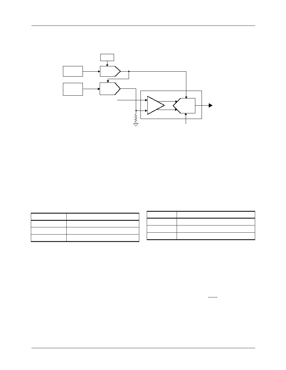
Analog-to-Digital Converter
Figure 2 is a block diagram of the ADC core with gain and
offset functions. G7-0, OS5-0, RGBIN and PD7-0 generically
refer to the gain and offset register values, analog input and
parallel data output of any RGB channel.
Within the A/D converter core are the following elements:
1.
Differential track and hold.
2.
Differential analog-to-digital converter.
Setting the gain register value G7-0 (GR7-0, GG7-0, GB7-0),
establishes the gain D/A converter voltage which is the upper
A/D reference voltage. Increasing the gain register value
reduces the output level. Conversion range is dened by the gain
setting according to Table 2.
Table 2. Gain Calibration
A/D Converter sensitivity is:
Offset is set through the Track and Hold which translates the
ground referenced input to a differential voltage centered
around A/D common mode bias voltage.
The 6-bit Offset D/A converter injects a current into RLEVEL
with two components:
1.
IBIAS to establish the A/D common mode voltage.
2.
IOFFSET to set the offset from the common mode level.
Voltage offset from the common mode voltage at the invert-
ing input of the Track and Hold is:
D/A converter gain tracks A/D gain with 1 LSB of offset cor-
responding to 1LSB of gain. Increasing the offset of a video
signal increases brightness of the picture. Data output from
the A/D converter is:
Impact of the offset values OSR5-0, OSG5-0, and OSB5-0 is
shown in Table 3.
Table 3. Offset Calibration
Sampling Clock PHASE Adjustment
PC generated image quality is strongly impacted by the
PHASE4-0 value. If PHASE is not set correctly, any section
of an image consisting of vertical lines may exhibit tearing.
Figure 3 shows how an analog input, VIN is sampled by the
rising edge of SCK after a delay PHASE from the rising
edge of either PXCK or XCK. SCK can be delayed up to 32
steps in 11.25° increments by adjusting the register value,
PHASE4-0.
Output data and clocks: DCK and DCK are delayed in tan-
dem with SCK relative to PXCK or XCK. There is a 5-51/2
clock latency between the data sample Sn and the corre-
sponding data out DA7-0.
G7-0
Conversion Range (mV)
0
500
102
700
255
1000
S
255
500
---------
=
255
G
70
–
+
-----------------------------LSB mV
V
OS
50
–
31
–
()
255
G
70
–
+
255
-----------------------------
500
255
---------
=
OS5-0
Equivalent Offset (bits)
0
-31d
31
0
63
32d
D
70
–
SV
IN
OS
50
–
31
–
()
–
=
Figure 2. A/D Converter Architecture
A/D
PD7-0
RGBIN
+
-
D/A
Current
D/A
Gain
Register
Offset
Register
RLEVEL
VOS
SCK
IBIAS + IOFFSET
VREF
G7-0
OS5-0
Track &
Hold
A/D Core
相关PDF资料 |
PDF描述 |
|---|---|
| FMS9875KGC100 | 3-CH 8-BIT PROPRIETARY METHOD ADC, PARALLEL ACCESS, PQFP100 |
| FMS9875KGC100X | 3-CH 8-BIT PROPRIETARY METHOD ADC, PARALLEL ACCESS, PQFP100 |
| FMS9875KGC140 | 3-CH 8-BIT PROPRIETARY METHOD ADC, PARALLEL ACCESS, PQFP100 |
| FMS9875KGC140X | 3-CH 8-BIT PROPRIETARY METHOD ADC, PARALLEL ACCESS, PQFP100 |
| FN3410-10-44 | 500 V, 50 HZ, THREE PHASE EMI FILTER |
相关代理商/技术参数 |
参数描述 |
|---|---|
| FMS9874KGC | 功能描述:视频 IC RoHS:否 制造商:Fairchild Semiconductor 工作电源电压:5 V 电源电流:80 mA 最大工作温度:+ 85 C 封装 / 箱体:TSSOP-28 封装:Reel |
| FMS9874KGC100 | 制造商:FAIRCHILD 制造商全称:Fairchild Semiconductor 功能描述:Graphics Digitizer - 3x8-Bit, 108Ms/s Triple Video A/D Converter with Clamps |
| FMS9875 | 制造商:FAIRCHILD 制造商全称:Fairchild Semiconductor 功能描述:Triple 8-Bit, 108/140 MHz A/D Converter with Clamps and PLL |
| FMS9875KAC100 | 制造商:FAIRCHILD 制造商全称:Fairchild Semiconductor 功能描述:Triple 8-Bit, 108/140 MHz A/D Converter with Clamps and PLL |
| FMS9875KAC140 | 制造商:FAIRCHILD 制造商全称:Fairchild Semiconductor 功能描述:Triple 8-Bit, 108/140 MHz A/D Converter with Clamps and PLL |
发布紧急采购,3分钟左右您将得到回复。