- 您现在的位置:买卖IC网 > PDF目录67505 > FMS9875KGC140 (FAIRCHILD SEMICONDUCTOR CORP) 3-CH 8-BIT PROPRIETARY METHOD ADC, PARALLEL ACCESS, PQFP100 PDF资料下载
参数资料
| 型号: | FMS9875KGC140 |
| 厂商: | FAIRCHILD SEMICONDUCTOR CORP |
| 元件分类: | ADC |
| 英文描述: | 3-CH 8-BIT PROPRIETARY METHOD ADC, PARALLEL ACCESS, PQFP100 |
| 封装: | MQFP-100 |
| 文件页数: | 3/31页 |
| 文件大小: | 517K |
| 代理商: | FMS9875KGC140 |
第1页第2页当前第3页第4页第5页第6页第7页第8页第9页第10页第11页第12页第13页第14页第15页第16页第17页第18页第19页第20页第21页第22页第23页第24页第25页第26页第27页第28页第29页第30页第31页
FMS9875
PRODUCT SPECIFICATION
REV. 1.2.15 1/14/02
11
Within the A/D converter core are the following elements:
1.
Differential track and hold.
2.
Differential analog-to-digital converter.
Setting the gain register value G7-0 (GRP7-0, GGY7-0, GBP7-0),
establishes the gain D/A converter voltage which is the upper
A/D reference voltage. Increasing the gain register value
reduces the output level. Conversion range is dened by the gain
setting according to Table 5.
Table 5. Gain Calibration
A/D Converter sensitivity is:
Offset is set through the Track and Hold, which translates the
ground referenced input to a differential voltage centered
around A/D common mode bias voltage.
The 6-bit Offset D/A converter injects a current into RLEVEL
with two components:
1.
IBIAS to establish the A/D common mode voltage.
2.
IOFFSET to set the offset from the common mode level.
Voltage offset from the common mode voltage at the invert-
ing input of the Track and Hold is:
D/A converter gain tracks A/D gain with 1 LSB of offset
corresponding to 1LSB of gain. Increasing the offset of a
video signal increases brightness of the picture. Data output
from the A/D converter is:
Impact of the offset values OSGY5-0, OSBP5-0, and OSRP5-0
is shown in Table 6.
Table 6. Offset Calibration
Sampling Clock PHASE Adjustment
Bandwidth of TV video is typically well below the horizon-
tal sampling rate. Consequently, PHASE has little impact on
images sampled in the YPBPR format or RGB signals derived
from a video source. By contrast, PC-generated image
quality is strongly impacted by the PHASE4-0 value. If
PHASE is not set correctly, any section of an image
consisting of vertical lines may exhibit tearing.
Figure 3 shows how an analog input, VIN is sampled by the
rising edge of SCK after a delay PHASE from the rising
edge of either PXCK or XCK. SCK can be delayed up to 32
steps in 11.25° increments by adjusting the register value,
PHASE4-0.
G7-0
Conversion Range (mV)
0
500
102
700
255
1000
S
255
500
---------
=
255
G
70
–
+
-----------------------------LSB mV
OS5-0
Equivalent Offset (bits)
0
-31d
31
0
63
32d
V
OS
50
–
31
–
()
255
G
70
–
+
255
-----------------------------
500
255
---------
=
D
70
–
SV
IN
OS
50
–
31
–
()
–
=
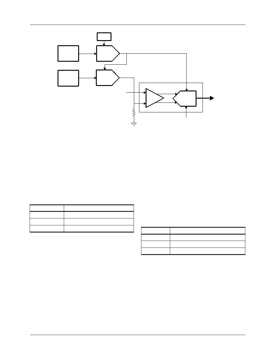
Figure 2. A/D Converter Architecture
A/D
D7-0
VIN
+
-
D/A
Current
D/A
Gain
Register
Offset
Register
RLEVEL
SCK
IBIAS + IOFFSET
VREF
G7-0
OS5-0
Track &
Hold
A/D Core
相关PDF资料 |
PDF描述 |
|---|---|
| FMS9875KGC140X | 3-CH 8-BIT PROPRIETARY METHOD ADC, PARALLEL ACCESS, PQFP100 |
| FN3410-10-44 | 500 V, 50 HZ, THREE PHASE EMI FILTER |
| FN3410-110-35 | 500 V, 50 HZ, THREE PHASE EMI FILTER |
| FN3410-13-44 | 500 V, 50 HZ, THREE PHASE EMI FILTER |
| FN3410-150-40 | 500 V, 50 HZ, THREE PHASE EMI FILTER |
相关代理商/技术参数 |
参数描述 |
|---|---|
| FMS9875KGC140X | 制造商:未知厂家 制造商全称:未知厂家 功能描述: |
| FMS9875KWC | 制造商:Fairchild Semiconductor Corporation 功能描述: |
| FMS9884A | 制造商:FAIRCHILD 制造商全称:Fairchild Semiconductor 功能描述:3x8-Bit, 108/140/175 Ms/s Triple Video A/D Converter with Clamps |
| FMS9884AKAC100 | 功能描述:视频模拟/数字化转换器集成电路 MQFP RoHS:否 制造商:Texas Instruments 输入信号类型:Differential 转换器数量:1 ADC 输入端数量:4 转换速率:3 Gbps 分辨率:8 bit 结构: 输入电压:3.3 V 接口类型:SPI 信噪比: 电压参考: 电源电压-最大:3.45 V 电源电压-最小:3.15 V 最大功率耗散: 最大工作温度:+ 85 C 最小工作温度:- 40 C 封装 / 箱体:TCSP-48 封装:Reel |
| FMS9884AKAC140 | 功能描述:视频模拟/数字化转换器集成电路 MQFP RoHS:否 制造商:Texas Instruments 输入信号类型:Differential 转换器数量:1 ADC 输入端数量:4 转换速率:3 Gbps 分辨率:8 bit 结构: 输入电压:3.3 V 接口类型:SPI 信噪比: 电压参考: 电源电压-最大:3.45 V 电源电压-最小:3.15 V 最大功率耗散: 最大工作温度:+ 85 C 最小工作温度:- 40 C 封装 / 箱体:TCSP-48 封装:Reel |
发布紧急采购,3分钟左右您将得到回复。