- 您现在的位置:买卖IC网 > PDF目录21524 > FOD3120SV (Fairchild Optoelectronics Group)OPTOCOUPLER GATE DRV 2.5A 8-SMD PDF资料下载
参数资料
| 型号: | FOD3120SV |
| 厂商: | Fairchild Optoelectronics Group |
| 文件页数: | 6/22页 |
| 文件大小: | 0K |
| 描述: | OPTOCOUPLER GATE DRV 2.5A 8-SMD |
| 标准包装: | 50 |
| 系列: | OPTOPLANAR® |
| 电压 - 隔离: | 5000Vrms |
| 通道数: | 1,单向 |
| 电流 - 输出 / 通道: | 2.5A |
| 传输延迟高 - 低 @ 如果: | 275ns @ 7mA ~ 16mA |
| 电流 - DC 正向(If): | 25mA |
| 输入类型: | DC |
| 输出类型: | 栅极驱动器 |
| 安装类型: | 表面贴装 |
| 封装/外壳: | 8-SMD,鸥翼型 |
| 供应商设备封装: | 8-SMDIP-W |
| 包装: | 管件 |
�� �
�
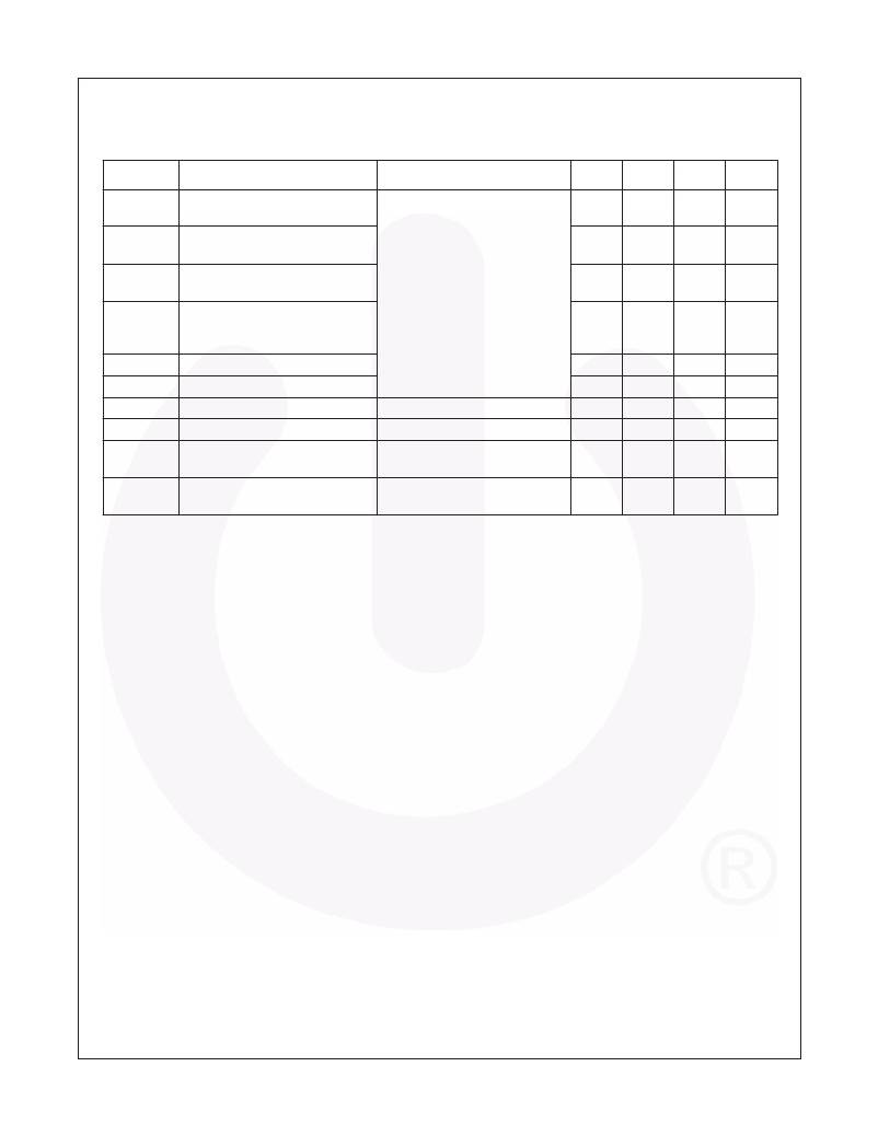
�Switching� Characteristics�
�Apply� over� all� recommended� conditions,� typical� value� is� measured� at� V� CC� =� 30V,� V� EE� =� Ground,� T� A� =� 25°C�
�unless� otherwise� speci?ed.�
�Symbol�
�Parameter�
�Conditions�
�Min.�
�Typ.�
�Max.�
�Units�
�t� PHL�
�t� PLH�
�Propagation� Delay� Time� to� Logic� I� F� =� 7mA� to� 16mA,�
�Low� Output� Rg� =� 10� ?� ,� Cg� =10nF,�
�Propagation� Delay� Time� to� Logic� f� =� 10kHz,� Duty� Cycle� =� 50%�
�150�
�150�
�275�
�255�
�400�
�400�
�ns�
�ns�
�High� Output�
�PWD�
�Pulse� Width� Distortion,�
�20�
�100�
�ns�
�|� t� PHL� –� t� PLH� |�
�PDD�
�Propagation� Delay� Difference�
�-250�
�250�
�ns�
�(Skew)�
�Between� Any� Two� Parts� or�
�Channels,� (t� PHL� –� t� PLH� )� (7)�
�t� r�
�t� f�
�Output� Rise� Time� (10%� –� 90%)�
�Output� Fall� Time� (90%� –� 10%)�
�60�
�60�
�ns�
�ns�
�t� UVLO� ON�
�t� UVLO� OFF�
�UVLO� Turn� On� Delay�
�UVLO� Turn� Off� Delay�
�I� F� =� 10mA� ,� V� O� >� 5V�
�I� F� =� 10mA� ,� V� O� <� 5V�
�1.6�
�0.4�
�μs�
�μs�
�|� CM� H� |�
�|� CM� L� |�
�Common� Mode� Transient�
�Immunity� at� Output� High�
�Common� Mode� Transient�
�Immunity� at� Output� Low�
�T� A� =� 25°C,� V� CC� =� 30V,�
�I� F� =� 7� to� 16mA,� V� CM� =� 2000V� (8)�
�T� A� =� 25°C,� V� CC� =� 30V,� V� F� =� 0V,�
�V� CM� =� 2000V� (9)�
�35�
�35�
�50�
�50�
�kV/μs�
�kV/μs�
�Notes:�
�1.� Maximum� pulse� width� =� 10μs,� maximum� duty� cycle� =� 1.1%�
�2.� Derate� linearly� above� 87°C,� free� air� temperature� at� a� rate� of� 0.77mW/°C�
�3.� No� derating� required� across� temperature� range.�
�4.� Functional� operation� under� these� conditions� is� not� implied.� Permanent� damage� may� occur� if� the� device� is�
�subjected� to� conditions� outside� these� ratings.�
�5.� Device� is� considered� a� two� terminal� device:� Pins� 2� and� 3� are� shorted� together� and� Pins� 5,� 6,� 7� and� 8� are� shorted�
�together.�
�6.� 5,000� V� RMS� for� 1� minute� duration� is� equivalent� to� 6,000� VAC� RMS� for� 1� second� duration.�
�7.� The� difference� between� t� PHL� and� t� PLH� between� any� two� FOD3120� parts� under� same� test� conditions.�
�8.� Common� mode� transient� immunity� at� output� high� is� the� maximum� tolerable� negative� dVcm/dt� on� the� trailing� edge� of�
�the� common� mode� impulse� signal,� Vcm,� to� assure� that� the� output� will� remain� high� (i.e.� V� O� >� 15.0V).�
�9.� Common� mode� transient� immunity� at� output� low� is� the� maximum� tolerable� positive� dVcm/dt� on� the� leading� edge� of�
�the� common� pulse� signal,� Vcm,� to� assure� that� the� output� will� remain� low� (i.e.� V� O� <� 1.0V).�
�10.� Pulse� Width,� P� W� ≤� 1μs,� 300pps�
�11.� Exponential� Waveform,� I� O(PEAK)� ≤� |� 2.5A� |� (� ≤� 0.3μs)�
�?2003� Fairchild� Semiconductor� Corporation�
�FOD3120� Rev.� 1.17.0�
�6�
�www.fairchildsemi.com�
�相关PDF资料 |
PDF描述 |
|---|---|
| FOD3120T | OPTOCOUPLER GATE DRV 2.5A 8-DIP |
| FOD3180V | OPTOCOUPLER HS 20V 2A VDE 8-DIP |
| FOD3180SV | OPTOCOUPLER HS 20V 2A VDE 8-SMD |
| 3385-7600 | SOCKET CONN 14 CONT CLOSED W/POL |
| FOD3150TSR2 | OPTOCOUPLER GATE DRV 1A 8-SMDIP |
相关代理商/技术参数 |
参数描述 |
|---|---|
| FOD3120T | 功能描述:逻辑输出光电耦合器 Optocoupl Logic-Out Push-Pul DC-In 1-Ch RoHS:否 制造商:Fairchild Semiconductor 绝缘电压:4243 Vrms 输出类型:Push-Pull 最大传播延迟时间:500 ns 最大正向二极管电压: 最大反向二极管电压: 最大正向二极管电流: 最大连续输出电流:2.5 A 最大功率耗散:100 mW 最大工作温度:+ 100 C 最小工作温度:- 40 C 封装 / 箱体:SO-16 封装:Tube |
| FOD3120TS | 功能描述:逻辑输出光电耦合器 Hi-Noise Immunity 2.5A Output RoHS:否 制造商:Fairchild Semiconductor 绝缘电压:4243 Vrms 输出类型:Push-Pull 最大传播延迟时间:500 ns 最大正向二极管电压: 最大反向二极管电压: 最大正向二极管电流: 最大连续输出电流:2.5 A 最大功率耗散:100 mW 最大工作温度:+ 100 C 最小工作温度:- 40 C 封装 / 箱体:SO-16 封装:Tube |
| FOD3120TSR2 | 功能描述:逻辑输出光电耦合器 High Noise Immunity 2.5A Out Gate RoHS:否 制造商:Fairchild Semiconductor 绝缘电压:4243 Vrms 输出类型:Push-Pull 最大传播延迟时间:500 ns 最大正向二极管电压: 最大反向二极管电压: 最大正向二极管电流: 最大连续输出电流:2.5 A 最大功率耗散:100 mW 最大工作温度:+ 100 C 最小工作温度:- 40 C 封装 / 箱体:SO-16 封装:Tube |
| FOD3120TSR2V | 功能描述:逻辑输出光电耦合器 High Noise Immunity 2.5A Out Gate RoHS:否 制造商:Fairchild Semiconductor 绝缘电压:4243 Vrms 输出类型:Push-Pull 最大传播延迟时间:500 ns 最大正向二极管电压: 最大反向二极管电压: 最大正向二极管电流: 最大连续输出电流:2.5 A 最大功率耗散:100 mW 最大工作温度:+ 100 C 最小工作温度:- 40 C 封装 / 箱体:SO-16 封装:Tube |
| FOD3120TSV | 功能描述:逻辑输出光电耦合器 High Noise Immunity 2.5A Output RoHS:否 制造商:Fairchild Semiconductor 绝缘电压:4243 Vrms 输出类型:Push-Pull 最大传播延迟时间:500 ns 最大正向二极管电压: 最大反向二极管电压: 最大正向二极管电流: 最大连续输出电流:2.5 A 最大功率耗散:100 mW 最大工作温度:+ 100 C 最小工作温度:- 40 C 封装 / 箱体:SO-16 封装:Tube |
发布紧急采购,3分钟左右您将得到回复。