参数资料
| 型号: | FOD4118 |
| 厂商: | Fairchild Semiconductor |
| 文件页数: | 4/12页 |
| 文件大小: | 0K |
| 描述: | TRIAC DRIVER ZERO CROSS 6-DIP |
| 产品目录绘图: | Opto 6-DIP Package |
| 标准包装: | 1,000 |
| 电压 - 隔离: | 5000Vrms |
| 通道数: | 1 |
| 电压 - 断路: | 800V |
| 输出类型: | 交流过零三端双向可控硅开关 |
| 电流 - 栅极触发电流 (Igt)(最大): | 1.3mA |
| 电流 - 保持 (Ih): | 200µA |
| 电流 - DC 正向(If): | 30mA |
| 电流 - 输出 / 通道: | 300mA |
| 安装类型: | 通孔 |
| 封装/外壳: | 6-DIP(0.300",7.62mm) |
| 供应商设备封装: | 6-DIP |
| 包装: | 管件 |
| 产品目录页面: | 2760 (CN2011-ZH PDF) |
| 其它名称: | FOD4118-ND FOD4118FS |
�� �
�
�Electrical� Characteristics� (T� A� =� 25°C� Unless� otherwise� specified)� (Continued)�
�Zero� Crossing� Characteristics�
�Symbol�
�V� INH�
�DC� Characteristics�
�Inhibit� Voltage� (MT1-MT2� voltage�
�Test� Conditions�
�I� F� =� Rated� I� FT�
�Min.�
�Typ.*�
�8�
�Max.�
�25�
�Units�
�V�
�above� which� device� will� not� trigger)�
�I� DRM2�
�Leakage� in� Inhibited� State�
�I� F� =� Rated� I� FT� ,�
�20�
�200�
�μA�
�Rated� V� DRM� ,� off� state�
�Isolation� Characteristics�
�Symbol�
�V� ISO�
�Characteristics�
�Input-Output� Isolation�
�Test� Conditions�
�(5)�
�f� =� 60Hz,� t� =� 1� min.�
�Min.�
�5000�
�Typ.*�
�Max.�
�Units�
�Vac(rms)�
�Voltage�
�*Typical� values� at� T� A� =� 25°C�
�Notes:�
�2.� Test� voltage� must� be� applied� within� dv/dt� rating.�
�3.� All� devices� are� guaranteed� to� trigger� at� an� I� F� value� less� than� or� equal� to� max� I� FT� .� Therefore,� recommended� operating�
�I� F� lies� between� max� I� FT� (2mA� for� FOD410� and� FOD4108� and� 1.3mA� for� FOD4116� and� FOD4118� and� the� absolute�
�max� I� F� (60mA).�
�4.� This� is� static� dv/dt.� See� Figure� 11� for� test� circuit.� Commutating� dv/dt� is� a� function� of� the� load-driving� thyristor(s)� only.�
�5.� Isolation� voltage,� V� ISO� ,� is� an� internal� device� dielectric� breakdown� rating.� For� this� test,� Pins� 1,� 2� and� 3� are� common,�
�and� Pins� 4,� 5� and� 6� are� common.�
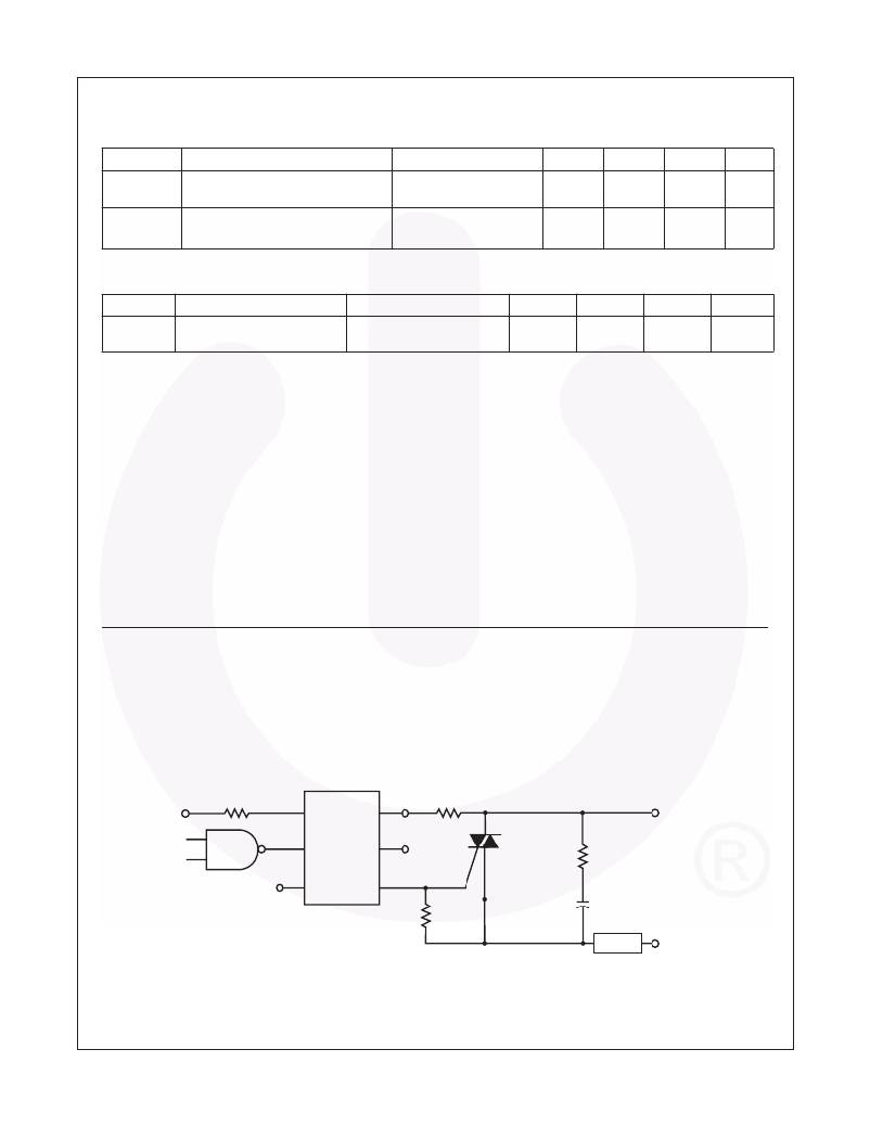
�Typical� Application�
�Typical� circuit� for� use� when� hot� line� switching� is� required.�
�In� this� circuit� the� “hot”� side� of� the� line� is� switched� and� the�
�load� connected� to� the� cold� or� neutral� side.� The� load� may�
�be� connected� to� either� the� neutral� or� hot� line.�
�R� in� is� calculated� so� that� I� F� is� equal� to� the� rated� I� FT� of� the�
�part,� 2mA� for� FOD410� and� FOD4108,� 1.3mA� for�
�FOD4116� and� FOD4118.� The� 39� ?� resistor� and� 0.01μF�
�capacitor� are� for� snubbing� of� the� triac� and� may� or� may�
�not� be� necessary� depending� upon� the� particular� triac�
�and� load� use.�
�V� CC�
�R� in�
�1�
�6�
�360� ?�
�HOT�
�2�
�FOD410�
�FOD4108�
�5�
�FKPF12N80�
�3�
�FOD4116�
�FOD4118�
�4�
�39*� ?�
�240� VAC�
�330� ?�
�0.01� μ� F�
�*� For� highly� inductive� loads� (power� factor� <� 0.5),� change� this� value� to� 360� ohms.�
�Figure� 1.� Hot-Line� Switching� Application� Circuit�
�LOAD�
�NEUTRAL�
�?2004� Fairchild� Semiconductor� Corporation�
�FOD410,� FOD4108,� FOD4116,� FOD4118� Rev.� 1.5.0�
�4�
�www.fairchildsemi.com�
�相关PDF资料 |
PDF描述 |
|---|---|
| 431002-09-0 | TERM BARRIER 9CIRC SGL ROW .4375 |
| 1455R1601 | BOX ALUM 6.30X6.50X1.20" BL/NAT |
| OSTYK31614030 | CONN BARRIER STRIP 14CIRC 7.62MM |
| TB200-06SP | TERM BLK 20A 6CIRC UL CSA IEC CE |
| 1455L2201 | BOX ALUM 8.66X4.06X1.20" BL/NAT |
相关代理商/技术参数 |
参数描述 |
|---|---|
| FOD4118S | 功能描述:三极与 SCR 输出光电耦合器 Zero-Cross Triac Out Snubberless, 800V RoHS:否 制造商:Vishay Semiconductors 输出设备:PhotoTriac 每芯片的通道数量: 绝缘电压:3750 Vrms 正向电流:10 mA 正向电压:1.2 V 最大触发电流:10 mA 关断状态下输出电压-VDRM:600 V 最大连续输出电流: 零交叉电路: 封装:Reel |
| FOD4118SD | 功能描述:三极与 SCR 输出光电耦合器 Black Pkg Zero Cross Snubless Triac Drver RoHS:否 制造商:Vishay Semiconductors 输出设备:PhotoTriac 每芯片的通道数量: 绝缘电压:3750 Vrms 正向电流:10 mA 正向电压:1.2 V 最大触发电流:10 mA 关断状态下输出电压-VDRM:600 V 最大连续输出电流: 零交叉电路: 封装:Reel |
| FOD4118SDV | 功能描述:三极与 SCR 输出光电耦合器 Black Pkg Zero Cross Snubless Triac Drver RoHS:否 制造商:Vishay Semiconductors 输出设备:PhotoTriac 每芯片的通道数量: 绝缘电压:3750 Vrms 正向电流:10 mA 正向电压:1.2 V 最大触发电流:10 mA 关断状态下输出电压-VDRM:600 V 最大连续输出电流: 零交叉电路: 封装:Reel |
| FOD4118SV | 功能描述:三极与 SCR 输出光电耦合器 Zero-Cross Triac Out Snubberless, 800V RoHS:否 制造商:Vishay Semiconductors 输出设备:PhotoTriac 每芯片的通道数量: 绝缘电压:3750 Vrms 正向电流:10 mA 正向电压:1.2 V 最大触发电流:10 mA 关断状态下输出电压-VDRM:600 V 最大连续输出电流: 零交叉电路: 封装:Reel |
| FOD4118T | 功能描述:三极与 SCR 输出光电耦合器 Zero-Cross Triac Out Snubberless, 800V RoHS:否 制造商:Vishay Semiconductors 输出设备:PhotoTriac 每芯片的通道数量: 绝缘电压:3750 Vrms 正向电流:10 mA 正向电压:1.2 V 最大触发电流:10 mA 关断状态下输出电压-VDRM:600 V 最大连续输出电流: 零交叉电路: 封装:Reel |
发布紧急采购,3分钟左右您将得到回复。