- 您现在的位置:买卖IC网 > Datasheet目录433 > FQP20N06L (Fairchild Semiconductor)MOSFET N-CH 60V 21A TO-220 Datasheet资料下载
参数资料
| 型号: | FQP20N06L |
| 厂商: | Fairchild Semiconductor |
| 文件页数: | 2/8页 |
| 文件大小: | 0K |
| 描述: | MOSFET N-CH 60V 21A TO-220 |
| 产品培训模块: | High Voltage Switches for Power Processing |
| 标准包装: | 50 |
| 系列: | QFET™ |
| FET 型: | MOSFET N 通道,金属氧化物 |
| FET 特点: | 逻辑电平门 |
| 漏极至源极电压(Vdss): | 60V |
| 电流 - 连续漏极(Id) @ 25° C: | 21A |
| 开态Rds(最大)@ Id, Vgs @ 25° C: | 55 毫欧 @ 10.5A,10V |
| Id 时的 Vgs(th)(最大): | 2.5V @ 250µA |
| 闸电荷(Qg) @ Vgs: | 13nC @ 5V |
| 输入电容 (Ciss) @ Vds: | 630pF @ 25V |
| 功率 - 最大: | 53W |
| 安装类型: | 通孔 |
| 封装/外壳: | TO-220-3 |
| 供应商设备封装: | TO-220 |
| 包装: | 管件 |
�� �
�
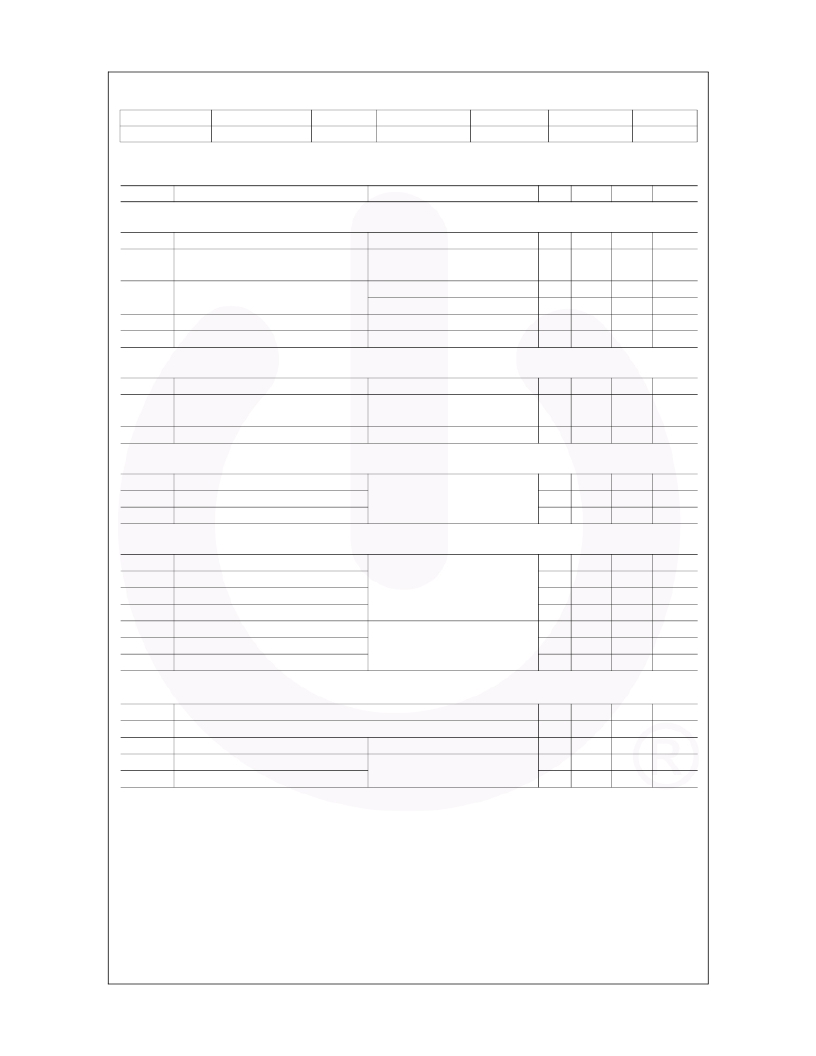
�Package� Marking� and� Ordering� Information�
�Part� Number�
�FQP20N06L�
�Top� Mark�
�FQP20N06L�
�Package�
�TO-220�
�Packing� Method�
�Tube�
�Reel� Size�
�N/A�
�Tape� Width�
�N/A�
�Quantity�
�50� units�
�Electrical� Characteristics�
�T� C� =� 25°C� unless� otherwise� noted.�
�Symbol�
�Parameter�
�Test� Conditions�
�Min�
�Typ�
�Max�
�Unit�
�Off� Characteristics�
�BV� DSS�
�Δ� BV� DSS�
�/� Δ� T� J�
�I� DSS�
�I� GSSF�
�I� GSSR�
�Drain-Source� Breakdown� Voltage�
�Breakdown� Voltage� Temperature�
�Coefficient�
�Zero� Gate� Voltage� Drain� Current�
�Gate-Body� Leakage� Current,� Forward�
�Gate-Body� Leakage� Current,� Reverse�
�V� GS� =� 0� V,� I� D� =� 250� μ� A�
�I� D� =� 250� μ� A,� Referenced� to� 25°C�
�V� DS� =� 60� V,� V� GS� =� 0� V�
�V� DS� =� 48� V,� T� C� =� 150°C�
�V� GS� =� 20� V,� V� DS� =� 0� V�
�V� GS� =� -20� V,� V� DS� =� 0� V�
�60�
�--�
�--�
�--�
�--�
�--�
�--�
�0.06�
�--�
�--�
�--�
�--�
�--�
�--�
�1�
�10�
�100�
�-100�
�V�
�V/°C�
�μ� A�
�μ� A�
�nA�
�nA�
�On� Characteristics�
�V� GS(th)�
�R� DS(on)�
�g� FS�
�Gate� Threshold� Voltage�
�Static� Drain-Source�
�On-Resistance�
�Forward� Transconductance�
�V� DS� =� V� GS� ,� I� D� =� 250� μ� A�
�V� GS� =� 10� V,� I� D� =� 10.5� A�
�V� GS� =� 5� V,� I� D� =10.5� A�
�V� DS� =� 25� V,� I� D� =� 10.5� A�
�1.0�
�--�
�--�
�--�
�--�
�0.042�
�0.055�
�11�
�2.5�
�0.055�
�0.07�
�--�
�V�
�Ω�
�S�
�Dynamic� Characteristics�
�C� iss�
�C� oss�
�C� rss�
�Input� Capacitance�
�Output� Capacitance�
�Reverse� Transfer� Capacitance�
�V� DS� =� 25� V,� V� GS� =� 0� V,�
�f� =� 1.0� MHz�
�--�
�--�
�--�
�480�
�175�
�35�
�630�
�230�
�45�
�pF�
�pF�
�pF�
�Switching� Characteristics�
�t� d(on)�
�t� r�
�t� d(off)�
�t� f�
�Q� g�
�Q� gs�
�Q� gd�
�Turn-On� Delay� Time�
�Turn-On� Rise� Time�
�Turn-Off� Delay� Time�
�Turn-Off� Fall� Time�
�Total� Gate� Charge�
�Gate-Source� Charge�
�Gate-Drain� Charge�
�V� DD� =� 30� V,� I� D� =� 10.5� A,�
�R� G� =� 25� Ω�
�V� DS� =� 48� V,� I� D� =� 21� A,�
�V� GS� =� 5� V�
�(Note� 4)�
�(Note� 4)�
�--�
�--�
�--�
�--�
�--�
�--�
�--�
�10�
�165�
�35�
�70�
�9.5�
�2.5�
�5.5�
�30�
�340�
�80�
�150�
�13�
�--�
�--�
�ns�
�ns�
�ns�
�ns�
�nC�
�nC�
�nC�
�Drain-Source� Diode� Characteristics� and� Maximum� Ratings�
�I� S�
�I� SM�
�Maximum� Continuous� Drain-Source� Diode� Forward� Current�
�Maximum� Pulsed� Drain-Source� Diode� Forward� Current�
�--�
�--�
�--�
�--�
�21�
�84�
�A�
�A�
�V� SD�
�t� rr�
�Q� rr�
�Drain-Source� Diode� Forward� Voltage�
�Reverse� Recovery� Time�
�Reverse� Recovery� Charge�
�V� GS� =� 0� V,� I� S� =� 21� A�
�V� GS� =� 0� V,� I� S� =� 21� A,�
�dI� F� /� dt� =� 100� A/� μ� s�
�--�
�--�
�--�
�--�
�54�
�75�
�1.5�
�--�
�--�
�V�
�ns�
�nC�
�Notes:�
�1.� Repetitive� Rating� :� Pulse� width� limited� by� maximum� junction� temperature.�
�2.� L� =� 450� μ� H,� I� AS� =� 21� A,� V� DD� =� 25� V,� R� G� =� 25� Ω,� starting� T� J� =� 25°C.�
�3.� I� SD� ≤� 21� A,� di/dt� ≤� 300� A� /μ� s,� V� DD� ≤� BV� DSS,� starting� T� J� =� 25°C.�
�4.� Essentially� independent� of� operating� temperature.�
�?2001� Fairchild� Semiconductor� Corporation�
�FQP20N06L� Rev.� C1�
�2�
�www.fairchildsemi.com�
�相关PDF资料 |
PDF描述 |
|---|---|
| FQP20N06TSTU | MOSFET N-CH 60V 20A TO-220 |
| FQP22N30 | MOSFET N-CH 300V 21A TO-220 |
| FQP24N08 | MOSFET N-CH 80V 24A TO-220 |
| FQP27N25 | MOSFET N-CH 250V 25.5A TO-220 |
| FQP27P06_SW82127 | MOSFET P-CH 60V 27A TO-220 |
相关代理商/技术参数 |
参数描述 |
|---|---|
| FQP20N06TSTU | 功能描述:MOSFET 60V N-Channel QFET Short Leads RoHS:否 制造商:STMicroelectronics 晶体管极性:N-Channel 汲极/源极击穿电压:650 V 闸/源击穿电压:25 V 漏极连续电流:130 A 电阻汲极/源极 RDS(导通):0.014 Ohms 配置:Single 最大工作温度: 安装风格:Through Hole 封装 / 箱体:Max247 封装:Tube |
| FQP22N30 | 功能描述:MOSFET 300V N-Channel QFET RoHS:否 制造商:STMicroelectronics 晶体管极性:N-Channel 汲极/源极击穿电压:650 V 闸/源击穿电压:25 V 漏极连续电流:130 A 电阻汲极/源极 RDS(导通):0.014 Ohms 配置:Single 最大工作温度: 安装风格:Through Hole 封装 / 箱体:Max247 封装:Tube |
| FQP22N30 | 制造商:Fairchild Semiconductor Corporation 功能描述:Transistor |
| FQP22P10 | 功能描述:MOSFET 100V P-Channel QFET RoHS:否 制造商:STMicroelectronics 晶体管极性:N-Channel 汲极/源极击穿电压:650 V 闸/源击穿电压:25 V 漏极连续电流:130 A 电阻汲极/源极 RDS(导通):0.014 Ohms 配置:Single 最大工作温度: 安装风格:Through Hole 封装 / 箱体:Max247 封装:Tube |
| FQP24N08 | 功能描述:MOSFET 80V N-Channel QFET RoHS:否 制造商:STMicroelectronics 晶体管极性:N-Channel 汲极/源极击穿电压:650 V 闸/源击穿电压:25 V 漏极连续电流:130 A 电阻汲极/源极 RDS(导通):0.014 Ohms 配置:Single 最大工作温度: 安装风格:Through Hole 封装 / 箱体:Max247 封装:Tube |
发布紧急采购,3分钟左右您将得到回复。