- 您现在的位置:买卖IC网 > PDF目录18447 > FQU6N40CTU_NBEA001 (Fairchild Semiconductor)MOSFET N-CH 400V 4.5A IPAK PDF资料下载
参数资料
| 型号: | FQU6N40CTU_NBEA001 |
| 厂商: | Fairchild Semiconductor |
| 文件页数: | 1/8页 |
| 文件大小: | 0K |
| 描述: | MOSFET N-CH 400V 4.5A IPAK |
| 标准包装: | 70 |
| 系列: | QFET™ |
| FET 型: | MOSFET N 通道,金属氧化物 |
| FET 特点: | 标准 |
| 漏极至源极电压(Vdss): | 400V |
| 电流 - 连续漏极(Id) @ 25° C: | 4.5A |
| 开态Rds(最大)@ Id, Vgs @ 25° C: | 1 欧姆 @ 2.25A,10V |
| Id 时的 Vgs(th)(最大): | 4V @ 250µA |
| 闸电荷(Qg) @ Vgs: | 20nC @ 10V |
| 输入电容 (Ciss) @ Vds: | 625pF @ 25V |
| 功率 - 最大: | 2.5W |
| 安装类型: | 通孔 |
| 封装/外壳: | TO-251-3 短引线,IPak,TO-251AA |
| 供应商设备封装: | I-Pak |
| 包装: | 管件 |
�� �
�
�November� 2013�
�FQD6N40C�
�N-Channel� QFET� ?� MOSFET�
�400� V,� 4.5� A,� 1.0� ?�
�Features�
�?� 4.5� A,� 400� V,� R� DS(on)� =� 1.0� Ω� (Max.)� @V� GS� =� 10� V,� I� D� =� 2.25� A�
�?� Low� Gate� Charge� (Typ.� 16� nC)�
�?� Low� Crss� (Typ.� 15� pF)�
�?� 100%� Avalanche� Tested�
�Description�
�This� N-Channel� enhancement� mode� power� MOSFET� is�
�produced� using� Fairchild� Semiconductor’s� proprietary�
�planar� stripe� and� DMOS� technology.� This� advanced�
�MOSFET� technology� has� been� especially� tailored� to� reduce�
�on-state� resistance,� and� to� provide� superior� switching�
�performance� and� high� avalanche� energy� strength.� These�
�devices� are� suitable� for� switched� mode� power� supplies,�
�active� power� factor� correction� (PFC),� and� electronic� lamp�
�ballasts.�
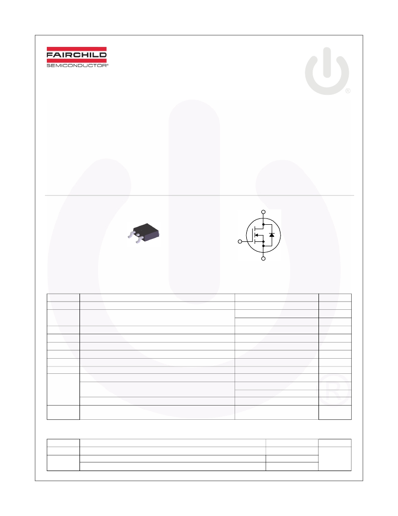
�D�
�D�
�G�
�S�
�D-PAK�
�G�
�S�
�Absolute� Maximum� Ratings�
�T� C� =� 25°C� unless� otherwise� noted.�
�Symbol�
�V� DSS�
�Drain-Source� Voltage�
�Parameter�
�FQD6N40CTM�
�400�
�Unit�
�V�
�I� D�
�Drain� Current�
�-� Continuous� (T� C� =� 25°C)�
�-� Continuous� (T� C� =� 100°C)�
�4.5�
�2.7�
�A�
�A�
�I� DM�
�Drain� Current�
�-� Pulsed�
�(Note� 1)�
�18�
�A�
�V� GSS�
�Gate-Source� Voltage�
�±� 30�
�V�
�E� AS�
�I� AR�
�E� AR�
�dv/dt�
�P� D�
�T� J� ,� T� STG�
�T� L�
�Single� Pulsed� Avalanche� Energy�
�Avalanche� Current�
�Repetitive� Avalanche� Energy�
�Peak� Diode� Recovery� dv/dt�
�Power� Dissipation� (T� A� =� 25°C)*�
�Power� Dissipation� (T� C� =� 25°C)�
�-� Derate� above� 25°C�
�Operating� and� Storage� Temperature� Range�
�Maximum� lead� temperature� for� soldering� purposes,�
�1/8� "� from� case� for� 5� seconds�
�(Note� 2)�
�(Note� 1)�
�(Note� 1)�
�(Note� 3)�
�270�
�4.5�
�4.8�
�4.5�
�2.5�
�48�
�0.38�
�-55� to� +150�
�300�
�mJ�
�A�
�mJ�
�V/ns�
�W�
�W�
�W/°C�
�°C�
�°C�
�Thermal� Characteristics�
�Symbol�
�R� θ� JC�
�R� θ� JA�
�Parameter�
�Thermal� Resistance,� Junction-to-Case,� Max.�
�Thermal� Resistance,� Junction-to-Ambient� (minimum� pad� of� 2� oz� copper),� Max.�
�Thermal� Resistance,� Junction-to-Ambient� (*� 1� in� 2� pad� of� 2� oz� copper),� Max.�
�FQD6N40CTM�
�2.6�
�110�
�50�
�Unit�
�°C� /� W�
�?2007� Fairchild� Semiconductor� Corporation�
�FQD6N40C� Rev.� C1�
�1�
�www.fairchildsemi.com�
�相关PDF资料 |
PDF描述 |
|---|---|
| ASG-C-X-B-10.000MHZ | OSC 10.00 MHZ 2.5V LVCMOS SMD |
| 3SS-WSP9-M7-KE | SWITCH PUSH SPST-NO 0.4VA 20V |
| FXO-HC730-19.44 | OSC 19.44 MHZ 3.3V HCMOS SMD |
| 3S1-SP9-B6-M7RE | SWITCH PUSH SPST-NO 0.4VA 20V |
| B32672L8472J289 | FILM CAP 4.7NF 5% 700VAC MKP |
相关代理商/技术参数 |
参数描述 |
|---|---|
| FQU6N50C | 制造商:FAIRCHILD 制造商全称:Fairchild Semiconductor 功能描述:These N-Channel enhancement mode power field effect transistors are produced using Fairchild’s proprietary planar stripe, DMOS technology |
| FQU6N50C_08 | 制造商:FAIRCHILD 制造商全称:Fairchild Semiconductor 功能描述:500V N-Channel MOSFET |
| FQU6N50CTU | 功能描述:MOSFET N-CH/500V/4.5A RoHS:否 制造商:STMicroelectronics 晶体管极性:N-Channel 汲极/源极击穿电压:650 V 闸/源击穿电压:25 V 漏极连续电流:130 A 电阻汲极/源极 RDS(导通):0.014 Ohms 配置:Single 最大工作温度: 安装风格:Through Hole 封装 / 箱体:Max247 封装:Tube |
| FQU6P25 | 制造商:FAIRCHILD 制造商全称:Fairchild Semiconductor 功能描述:250V P-Channel MOSFET |
| FQU6P25TU | 功能描述:MOSFET RoHS:否 制造商:STMicroelectronics 晶体管极性:N-Channel 汲极/源极击穿电压:650 V 闸/源击穿电压:25 V 漏极连续电流:130 A 电阻汲极/源极 RDS(导通):0.014 Ohms 配置:Single 最大工作温度: 安装风格:Through Hole 封装 / 箱体:Max247 封装:Tube |
发布紧急采购,3分钟左右您将得到回复。