- 您现在的位置:买卖IC网 > PDF目录79119 > FS1501-9RTB2 (POWER-ONE INC) 1-OUTPUT 100 W DC-DC REG PWR SUPPLY MODULE PDF资料下载
参数资料
| 型号: | FS1501-9RTB2 |
| 厂商: | POWER-ONE INC |
| 元件分类: | 电源模块 |
| 英文描述: | 1-OUTPUT 100 W DC-DC REG PWR SUPPLY MODULE |
| 封装: | METAL, CASE S02, MODULE |
| 文件页数: | 20/33页 |
| 文件大小: | 438K |
| 代理商: | FS1501-9RTB2 |
第1页第2页第3页第4页第5页第6页第7页第8页第9页第10页第11页第12页第13页第14页第15页第16页第17页第18页第19页当前第20页第21页第22页第23页第24页第25页第26页第27页第28页第29页第30页第31页第32页第33页
S Series Data Sheet
100 Watt AC-DC and DC-DC Converters
APR 26, 2006 revised to SEP 25, 2006
Page 27 of 33
www.power-one.com
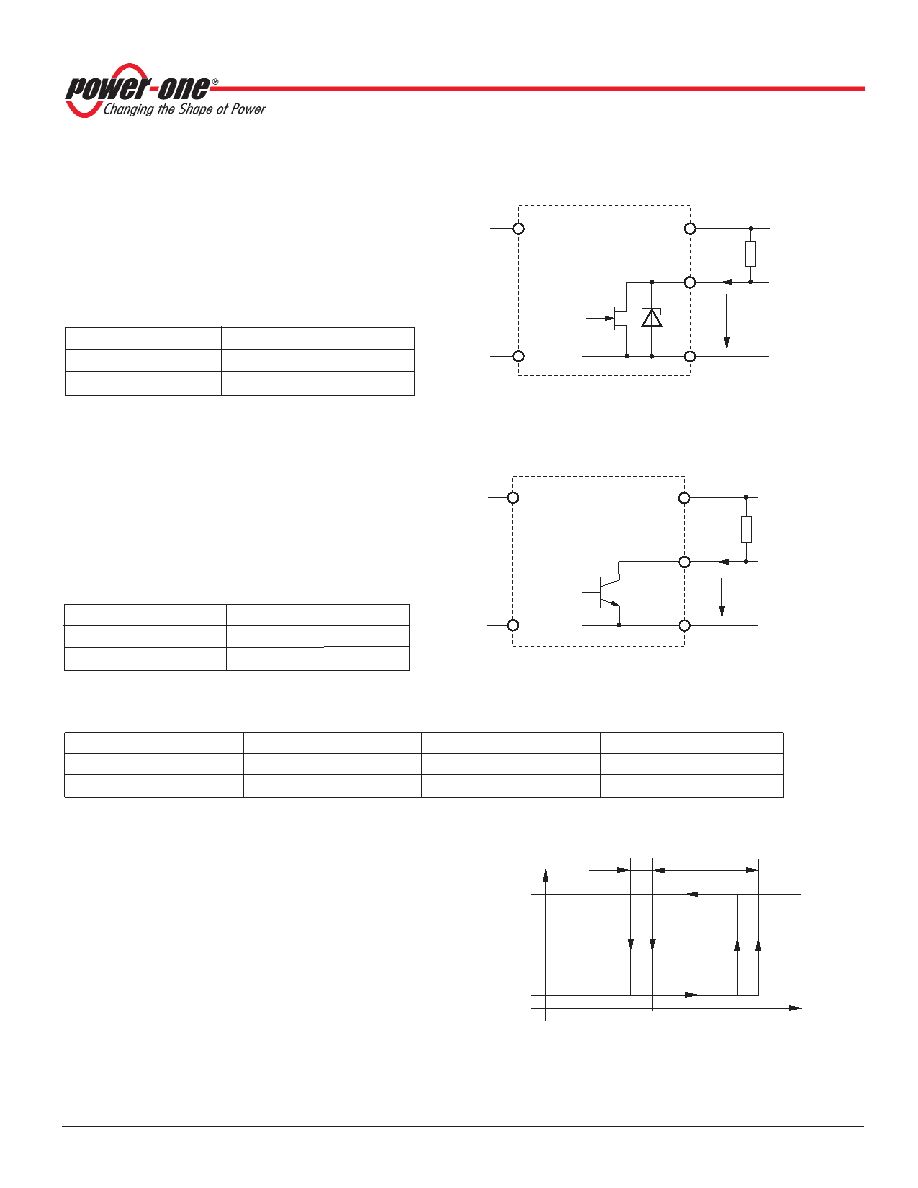
NPN output (D5 - DD):
Pin 20 (D) is internally connected via the collector-emitter
path of an NPN transistor to Vo1+ or Vo+. VD < 0.4 V
(logic low) corresponds to a monitored voltage level (Vi
and/or Vo1) > Vt +Vh. The current ID through pin 20
should not exceed 20 mA. This output is not protected
against external overvoltages. VD should not exceed 40 V.
Vi, Vo1 status
D output,
VD
Vi or Vo1 < Vt
high, H,
ID ≤ 25 A at VD = 40 V
Vi and Vo1 > Vt + Vh
low, L,
VD ≤ 0.4 V at ID = 20 mA
JFET output (D0 - D4):
Pin 20 (D) is internally connected via the drain-source path
of a JFET (self-conducting type) to Vo1+ or Vo+.
VD ≤ 0.4 V (logic low) corresponds to a monitored voltage
level (Vi and/or Vo1) < Vt. The current ID through the JFET
should not exceed 2.5 mA. The JFET is protected by a
0.5 W Zener diode of 8.2 V against external overvoltages.
Vi, Vo1 status
D output,
VD
Vi or Vo1 < Vt
low, L,
VD ≤ 0.4 V at ID = 2.5 mA
Vi and Vo1 > Vt + Vh
high, H,
ID ≤ 25 A at VD = 5.25 V
Fig. 31
Option D1 - D0: JFET output, ID ≤ 2.5 mA
Table 21: D-output logic signals
Version of D
Vi << Vt resp. Vo << Vt
Vi >> Vt + Vh resp. Vo >> Vt
Configuration
D1, D2, D3, D4, D0
low
high
JFET
D5, D6, D7, D8, D9, DD
high
low
NPN
Vo1+
Vo1–
D
VD
ID
Rp
Input
11007
Vo1+
Vo1–
D
VD
ID
Rp
Input
11006
Fig. 32
Option D5 - DD: NPN output, Vo1 ≤ 40 V, ID ≤ 20 mA
Threshold tolerances and hysteresis:
If Vi is monitored, the internal input voltage after the input
filter is measured. Consequently, this voltage differs from
the voltage at the connector pins by the voltage drop
ΔVti
across the input filter. The threshold levels of the D0 and
D9 options are factory-adjusted at nominal output current
Io nom and at TA = 25 °C. The value of ΔVti depends upon
the input voltage range (CS, DS, ..), threshold level Vt,
temperature and input current. The input current is a
function of the input voltage and the output power.
Fig. 33
Definition of Vti, ΔVt i and ΔVhi (JFET output)
ΔV
ti
Vhi
VD low
VD
VD high
Vi
P
o
=
P
o
nom
P
o
=
0
P
o
=
0
Vti
P
o
=
P
o
nom
11021
相关PDF资料 |
PDF描述 |
|---|---|
| FS1601-7ERD4B2 | 1-OUTPUT 100 W DC-DC REG PWR SUPPLY MODULE |
| FS1601-7ERD8B2 | 1-OUTPUT 100 W DC-DC REG PWR SUPPLY MODULE |
| FS1601-7PD5B2 | 1-OUTPUT 100 W DC-DC REG PWR SUPPLY MODULE |
| FS1601-9PD3B2 | 1-OUTPUT 100 W DC-DC REG PWR SUPPLY MODULE |
| FS1601-9RD9TB2 | 1-OUTPUT 100 W DC-DC REG PWR SUPPLY MODULE |
相关代理商/技术参数 |
参数描述 |
|---|---|
| FS150-20 | 制造商:JAMECO VALUEPRO 功能描述:Test Leads Breadboard 20 Pack 5.9 Inch (150mm) Wire Pin Cont |
| FS150AR | 制造商:Hammond Power Solutions 功能描述:Transformer, Control, 1ph, 150VA, 600-12x24V, 60Hz |
| FS150K.5AB3 | 制造商:TE Connectivity 功能描述: |
| FS150R06KE3 | 功能描述:IGBT 模块 IGBT MODULES 600V RoHS:否 制造商:Infineon Technologies 产品:IGBT Silicon Modules 配置:Dual 集电极—发射极最大电压 VCEO:600 V 集电极—射极饱和电压:1.95 V 在25 C的连续集电极电流:230 A 栅极—射极漏泄电流:400 nA 功率耗散:445 W 最大工作温度:+ 125 C 封装 / 箱体:34MM 封装: |
| FS150R07N3E4 | 制造商:Infineon Technologies AG 功能描述:IGBT Module 150A 650V |
发布紧急采购,3分钟左右您将得到回复。