参数资料
| 型号: | FS7140-02G-XTP |
| 厂商: | ON Semiconductor |
| 文件页数: | 15/17页 |
| 文件大小: | 0K |
| 描述: | IC CLOCK GEN PLL PROG 16SSOP |
| 标准包装: | 2,000 |
| 类型: | PLL 时钟发生器 |
| PLL: | 是 |
| 输入: | 晶体 |
| 输出: | CMOS,PECL |
| 电路数: | 1 |
| 比率 - 输入:输出: | 2:1 |
| 差分 - 输入:输出: | 无/是 |
| 频率 - 最大: | 400MHz |
| 除法器/乘法器: | 是/无 |
| 电源电压: | 3 V ~ 3.6 V |
| 工作温度: | 0°C ~ 70°C |
| 安装类型: | 表面贴装 |
| 封装/外壳: | 16-SSOP(0.209",5.30mm 宽) |
| 供应商设备封装: | 16-SSOP |
| 包装: | 带卷 (TR) |
FS7140, FS7145
http://onsemi.com
7
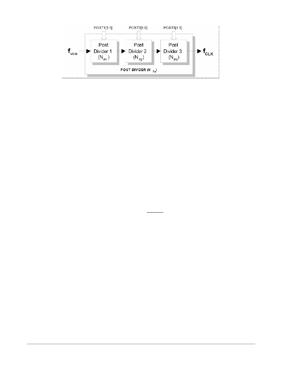
Figure 2. Post Divider
The moduli of the individual dividers are denoted as NP1,
NP2 and NP3, and together they make up the array modulus
NPX.
NPX = NP1 x NP2 x NP3
The post divider performs several useful functions. First,
it allows the VCO to be operated in a narrower range of
speeds compared to the variety of output clock speeds that
the device is required to generate. Second, the extra integer
in the denominator permits more flexibility in the
programming of the loop for many applications where
frequencies must be achieved exactly.
Note that a nominal 50/50 duty factor is always preserved
(even for selections which have an odd modulus).
See Table 12 for additional information.
Crystal Oscillator
The FS7140 is equipped with a Piercetype crystal
oscillator. The crystal is operated in parallel resonant mode.
Internal load capacitance is provided for the crystal. While
a recommended load capacitance for the crystal is specified,
crystals for other standard load capacitances may be used if
great precision of the reference frequency (100 ppm or less)
is not required.
Reference Divider Source MUX
The source of frequency for the reference divider can be
chosen to be the device crystal oscillator or the REF pin by
the REFDSRC bit.
When not using the crystal oscillator, it is preferred to
connect XIN to VSS. Do not connect to XOUT.
When not using the REF input, it is preferred to leave it
floating or connected to VDD.
Feedback Divider Source MUX
The source of frequency for the feedback divider may be
selected to be either the output of the post divider or the
output of the VCO by the FBKDSRC bit.
Ordinarily, for frequency synthesis, the output of the VCO
is used. Use the output of the post divider only where a
deterministic phase relationship between the output clock
and reference clock are desired (linelocked mode, for
example).
Device Shutdown
Two bits are provided to effect shutdown of the device if
desired, when it is not active. SHUT1 disables most
externally observable device functions. SHUT2 reduces
device quiescent current to absolute minimum values.
Normally, both bits should be set or cleared together.
Serial communications capability is not disabled by either
SHUT1 or SHUT2.
Differential Output Stage
The differential output stage supports both CMOS and
pseudoECL (PECL) signals. The desired output interface
is chosen via the programming registers.
If a PECL interface is used, the transmission line is usually
terminated using a Thévenin termination. The output stage
can only sink current in the PECL mode, and the amount of
sink current is set by a programming resistor on the
LOCK/IPRG pin. The ratio of output sink current to IPRG
current is 13:1. Source current for the CLKx pins is provided
by the pullup resistors that are part of the Thévenin
termination.
Example
Assume that it is desired to connect a PECLtype fanout
buffer right next to the FS7140.
Further assume:
VDD = 3.3 V
Desired VHI = 2.4 V
Desired VLO = 1.6 V
Equivalent RLOAD = 75 ohms
Then:
R1 (from CLKP and CLKN output to VDD) =
RLOAD * VDD / VHI =
75 * 3.3 / 2.4 =
103 ohms
R2 (from CLKP and CLKN output to GND) =
RLOAD * VDD / (VDD VHI) =
75 * 3.3 / (3.3 2.4) =
275 ohms
Rprgm (from VDD to IPRG pin) =
26 * (VDD * RLOAD) / (VHI VLO) / 3 =
26 * (3.3 * 75) / (2.4 1.6) / 3 =
2.68 Kohms
相关PDF资料 |
PDF描述 |
|---|---|
| VE-B1Y-MY-F3 | CONVERTER MOD DC/DC 3.3V 33W |
| VI-25F-MW-F1 | CONVERTER MOD DC/DC 72V 100W |
| M83723/95W2028N | CONN PLUG 28POS STRAIGHT W/SCKT |
| M83723/95W20281 | CONN PLUG 28POS STRAIGHT W/SCKT |
| GTC030F-36-52P | CONN RCPT 52POS PANEL MNT W/PINS |
相关代理商/技术参数 |
参数描述 |
|---|---|
| FS7140-802 | 制造商:AMI Semiconductor 功能描述: |
| FS7145 | 制造商:AMI 制造商全称:AMI 功能描述:Programmable Phase-Locked Loop Clock Generator |
| FS7145-01-XTD | 功能描述:时钟发生器及支持产品 I2C PLL CLOCK 3.3V RoHS:否 制造商:Silicon Labs 类型:Clock Generators 最大输入频率:14.318 MHz 最大输出频率:166 MHz 输出端数量:16 占空比 - 最大:55 % 工作电源电压:3.3 V 工作电源电流:1 mA 最大工作温度:+ 85 C 安装风格:SMD/SMT 封装 / 箱体:QFN-56 |
| FS7145-01-XTP | 功能描述:时钟发生器及支持产品 I2C PLL CLOCK 3.3V RoHS:否 制造商:Silicon Labs 类型:Clock Generators 最大输入频率:14.318 MHz 最大输出频率:166 MHz 输出端数量:16 占空比 - 最大:55 % 工作电源电压:3.3 V 工作电源电流:1 mA 最大工作温度:+ 85 C 安装风格:SMD/SMT 封装 / 箱体:QFN-56 |
| FS7145-02G | 制造商:ON Semiconductor 功能描述:PROGRAMMABLE PHASED-LOCKED-LOOP CLOCK GENERATOR, SSOP - Tape and Reel |
发布紧急采购,3分钟左右您将得到回复。