参数资料
| 型号: | FS7145-01-XTP |
| 厂商: | ON Semiconductor |
| 文件页数: | 14/17页 |
| 文件大小: | 0K |
| 描述: | IC PLL CLK GEN I2C PROGR 16-SOIC |
| 标准包装: | 3,000 |
| 类型: | PLL 时钟发生器 |
| PLL: | 是 |
| 输入: | 晶体 |
| 输出: | CMOS,PECL |
| 电路数: | 1 |
| 比率 - 输入:输出: | 2:1 |
| 差分 - 输入:输出: | 无/是 |
| 频率 - 最大: | 400MHz |
| 除法器/乘法器: | 是/无 |
| 电源电压: | 3 V ~ 3.6 V |
| 工作温度: | 0°C ~ 70°C |
| 安装类型: | 表面贴装 |
| 封装/外壳: | 16-SOIC(0.154",3.90mm 宽) |
| 供应商设备封装: | 16-SOIC N |
| 包装: | 带卷 (TR) |
FS7140, FS7145
http://onsemi.com
6
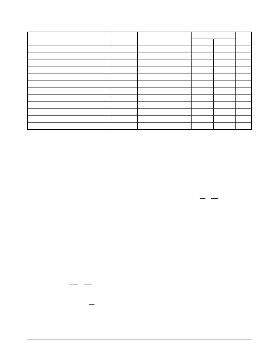
Table 6. SERIAL INTERFACE TIMING SPECIFICATIONS (Note 3)
Parameter
Symbol
Conditions/Description
Fast Mode
Units
Min
Max
Clock frequency
fSCL
SCL
0
400
kHz
Bus free time between STOP and START
tBUF
1300
ns
Setup time, START (repeated)
Tsu:STA
600
ns
Hold time, START
thd:STA
600
ns
Setup time, data input
Tsu:DAT
SDA
100
ns
Hold time, data input
thd:DAT
SDA
0
ns
Output data valid from clock
tAA
900
ns
Rise time, data and clock
tR
SDA, SCL
300
ns
Fall time, data and clock
tF
SDA, SCL
300
ns
High time, clock
tHI
SCL
600
ns
Low time, clock
tLO
SCL
1300
ns
Setup time, STOP
tsu:STO
600
ns
3. Unless otherwise stated, VDD = 3.3 V ± 10%, no load on any output, and ambient temperature range TA = 0°C to 70°C. Parameters denoted
with an asterisk (*) represent nominal characterization data and are not production tested to any specific limits. MIN and MAX characterization
data are ± 3s from typical.
FUNCTIONAL BLOCK DIAGRAM
Phase Locked Loop (PLL)
The PLL is a standard phase and frequencylocked loop
architecture. The PLL consists of a reference divider, a
phasefrequency detector (PFD), a charge pump, an internal
loop filter, a voltagecontrolled oscillator (VCO), a
feedback divider, and a post divider.
The reference frequency (generated by either the
onboard crystal oscillator or an external frequency source),
is first reduced by the reference divider. The integer value
that the frequency is divided by is called the modulus and is
denoted as NR for the reference divider. This divided
reference is then fed into the PFD.
The VCO frequency is fed back to the PFD through the
feedback divider (the modulus is denoted by NF).
The PFD will drive the VCO up or down in frequency until
the divided reference frequency and the divided VCO
frequency appearing at the inputs of the PFD are equal. The
input/output relationship between the reference frequency
and the VCO frequency is then:
fVCO
NF
+
fREF
NR
This basic PLL equation can be rewritten as
fVCO + fREF
NF
NR
A post divider (actually a series combination of three post
dividers) follows the PLL and the final equation for device
output frequency is:
fCLK + fREF
NF
NR
1
NPx
Reference Divider
The reference divider is designed for low phase jitter. The
divider accepts the output of either the crystal oscillator
circuit or an external reference frequency. The reference
divider is a 12 bit divider, and can be programmed for any
modulus from 1 to 4095 (divide by 1 not available on date
codes prior to 0108).
Feedback Divider
The feedback divider is based on a dualmodulus divider
(also called dualmodulus prescaler) technique. It permits
division by any integer value between 12 and 16383. Simply
program the FBKDIV register with the binary equivalent of
the desired modulus. Selected moduli below 12 are also
permitted. Moduli of: 4, 5, 8, 9, and 10 are also allowed (4
and 5 are not available on date codes prior to 0108).
Post Divider
The post divider consists of three individually
programmable dividers, as shown in Figure 2.
相关PDF资料 |
PDF描述 |
|---|---|
| VE-B6X-MV-F1 | CONVERTER MOD DC/DC 5.2V 150W |
| MAX5380MEUK+T | IC DAC 8BIT 2WIRE SER SOT23-5 |
| MS3456KS16S-1S | CONN PLUG 7POS STRAIGHT W/SCKT |
| D38999/20SD18SC | CONN RCPT 18POS WALL MNT W/SCKT |
| MS27496E25B61PA | CONN RCPT 61POS BOX MNT W/PINS |
相关代理商/技术参数 |
参数描述 |
|---|---|
| FS7145-02G | 制造商:ON Semiconductor 功能描述:PROGRAMMABLE PHASED-LOCKED-LOOP CLOCK GENERATOR, SSOP - Tape and Reel |
| FS7145-02G-XTD | 功能描述:时钟发生器及支持产品 FS7145-02G CLOCK ASSP SS RoHS:否 制造商:Silicon Labs 类型:Clock Generators 最大输入频率:14.318 MHz 最大输出频率:166 MHz 输出端数量:16 占空比 - 最大:55 % 工作电源电压:3.3 V 工作电源电流:1 mA 最大工作温度:+ 85 C 安装风格:SMD/SMT 封装 / 箱体:QFN-56 |
| FS7145-02G-XTP | 功能描述:时钟发生器及支持产品 FS7145-02G CLOCK ASSP SS RoHS:否 制造商:Silicon Labs 类型:Clock Generators 最大输入频率:14.318 MHz 最大输出频率:166 MHz 输出端数量:16 占空比 - 最大:55 % 工作电源电压:3.3 V 工作电源电流:1 mA 最大工作温度:+ 85 C 安装风格:SMD/SMT 封装 / 箱体:QFN-56 |
| FS714X | 制造商:ONSEMI 制造商全称:ON Semiconductor 功能描述:Programmable Phase-Locked Loop Clock Generator |
| FS7-4 | 制造商:未知厂家 制造商全称:未知厂家 功能描述:Flow Switches - Liquid |
发布紧急采购,3分钟左右您将得到回复。