- 您现在的位置:买卖IC网 > PDF目录68995 > FS8S0765RCTU (FAIRCHILD SEMICONDUCTOR CORP) 28 A SWITCHING REGULATOR, 150 kHz SWITCHING FREQ-MAX, PSFM5 PDF资料下载
参数资料
| 型号: | FS8S0765RCTU |
| 厂商: | FAIRCHILD SEMICONDUCTOR CORP |
| 元件分类: | 稳压器 |
| 英文描述: | 28 A SWITCHING REGULATOR, 150 kHz SWITCHING FREQ-MAX, PSFM5 |
| 封装: | TO-220, 5 PIN |
| 文件页数: | 3/19页 |
| 文件大小: | 1913K |
| 代理商: | FS8S0765RCTU |
FS8S0765RC
11
Function Information
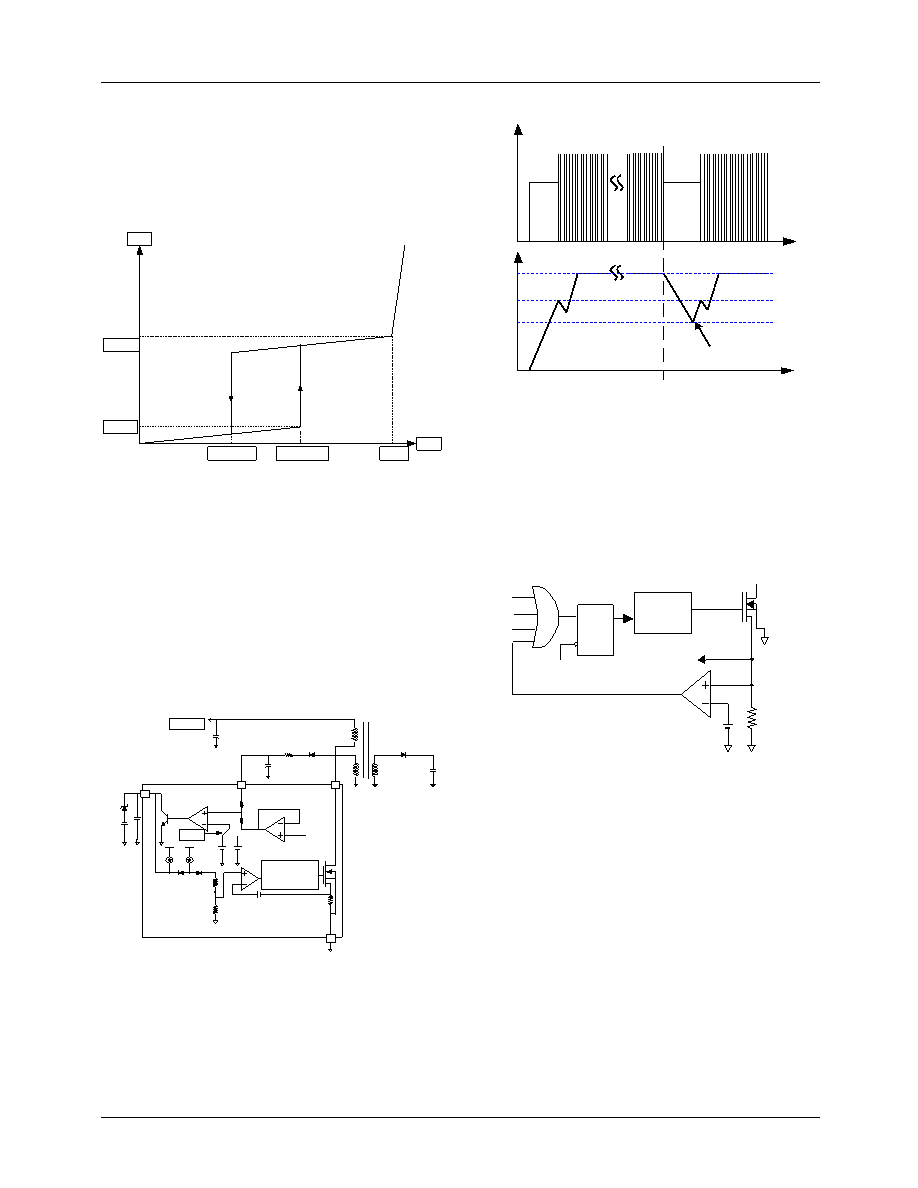
1. Start up circuit : To guarantee stable operation of the
control IC, the FS8S0765RC has the UVLO circuit with 6V
hysteresis. The Vcc start up voltage is 15V and the stop volt-
age is 9V. When the Vcc reaches 15V, the control IC oper-
ates. Once the control IC start operating, it continues to
operate until the Vcc is below the stop voltage, 9V.
Figure 1. Strat up with hysteresis
2. The primary side regulation : To control the transformer
output, the FPS compares the feedback voltage with the
current sensing voltage. To generate the feedback voltage,
the existing FPS uses the photo coupler and TL431, etc in the
secondary side regulation SMPS. But in the SMPS using the
FS8S0765RC, these components do not need. The regulation
circuit to control the feedback voltage is built in the control
IC as shown figure 2. During the normal operation, the Vcc
voltage is regulated to 22V by the Vcc reference voltage, V1.
And at burst mode, the Vcc voltage fluctuates between 11V
to 12V by the reference voltage, V2.
Figure 2. Circuit for the primary side regulation
3. Protection function : The FS8S0765RC has 3 self
protective functions(OCP, OLP and TSD). Because it does
not require the additional external components, the reliability
can be achieved without cost increase. These protection
functions operate in auto restart mode. The protection is reset
when the Vcc voltage goes below 9V. The control IC
operates again when the Vcc voltage is recharged to 15V.
Figure 3. Auto restart operation after protection
3.1 Over Current Protection(OCP) : Although the cycle by
cycle over current limit tries to limit the peak current to a
predetermined level, it can not work during the leading edge
blanking. When the secondary rectifying diodes or the
transformer pins are shorted, a steep current with extremely
high di/dt can flow during the leading edge blanking. The
OCP block is added to ensure the reliability. It turns off the
SenseFET within 300ns after the abnormal over current con-
dition is sensed.
Figure 4. OCP block
3.2 Over Load Protection(OLP) : During the over load
condition, the ouput of the internal error amp(Amp1) shown
in the figure 2 is zero. The feedback voltage, Vfb is charged
up by the internal current source of 2uA. When Vfb touches
7.5V, the OLP block is activated as shown in figure 5.
Vstop=9V
Vstart=15V
80uA
OVP
Vcc
Icc
15mA
Vc c
Vb i a s
V1
4
3
2u A
0.9mA
Cfb
D1
D2
Id elay
Ifb
Nv cc
Nv o
Gate driv er
Np
Vf b
F a ir child P o w e r S w itch (F S 8 S 0 765R C )
1
2
Dra in
GND
V2
Burs t
signa l
Cd
DC L ink
Vo l t ag e
Am p1
Am p2
time
V
15 V
9V
Vcc
Vds
P rotection opera ting
(O CP ,O L P or TS D )
A uto res ta rt
22 V
GATE
DRIVER
OCP COMP.
Vsense : 1V
SenseFET
S Q'
R
OVP
OLP
TSD
UVLO
PWMComp
相关PDF资料 |
PDF描述 |
|---|---|
| FS8S0765RCYDTU | 28 A SWITCHING REGULATOR, 150 kHz SWITCHING FREQ-MAX, PZFM5 |
| FSA2467MTCX | DUAL 2-CHANNEL, DBL POLE DBL THROW SWITCH, PDSO16 |
| FSAR001BNY | AC-DC REG PWR SUPPLY MODULE |
| FSBH0170NYF116 | 0.9 A SWITCHING CONTROLLER, 106 kHz SWITCHING FREQ-MAX, PDIP8 |
| FSBH0270NYF116 | 1.1 A SWITCHING CONTROLLER, 106 kHz SWITCHING FREQ-MAX, PDIP8 |
相关代理商/技术参数 |
参数描述 |
|---|---|
| FS8S0765RCYDTU | 制造商:未知厂家 制造商全称:未知厂家 功能描述:SMPS Controller |
| FS8S0965RCB | 制造商:FAIRCHILD 制造商全称:Fairchild Semiconductor 功能描述:Fairchild Power Switch(FPS) |
| FS8S0965RCBSYDT | 功能描述:电源开关 IC - 配电 FPS FOR CRT RoHS:否 制造商:Exar 输出端数量:1 开启电阻(最大值):85 mOhms 开启时间(最大值):400 us 关闭时间(最大值):20 us 工作电源电压:3.2 V to 6.5 V 电源电流(最大值): 最大工作温度:+ 85 C 安装风格:SMD/SMT 封装 / 箱体:SOT-23-5 |
| FS8S0965RCBTU | 制造商:FAIRCHILD 制造商全称:Fairchild Semiconductor 功能描述:Fairchild Power Switch(FPS) |
| FS8S0965RCBYDTU | 功能描述:电源开关 IC - 配电 9A/650V Snyc FPS Primary RoHS:否 制造商:Exar 输出端数量:1 开启电阻(最大值):85 mOhms 开启时间(最大值):400 us 关闭时间(最大值):20 us 工作电源电压:3.2 V to 6.5 V 电源电流(最大值): 最大工作温度:+ 85 C 安装风格:SMD/SMT 封装 / 箱体:SOT-23-5 |
发布紧急采购,3分钟左右您将得到回复。