参数资料
| 型号: | FSA2147K8X |
| 厂商: | Fairchild Semiconductor |
| 文件页数: | 4/10页 |
| 文件大小: | 0K |
| 描述: | IC SWITCH DUAL DPST US8 |
| 标准包装: | 1 |
| 功能: | 开关 |
| 电路: | 2 x DPST - NO |
| 导通状态电阻: | 3 欧姆 |
| 电压电源: | 单电源 |
| 电压 - 电源,单路/双路(±): | 2.7 V ~ 4.3 V |
| 工作温度: | -40°C ~ 85°C |
| 安装类型: | 表面贴装 |
| 封装/外壳: | 8-VFSOP(0.091",2.30mm 宽) |
| 供应商设备封装: | US8 |
| 包装: | 标准包装 |
| 产品目录页面: | 1218 (CN2011-ZH PDF) |
| 其它名称: | FSA2147K8XDKR |
2008 Fairchild Semiconductor Corporation
www.fairchildsemi.com
FSA2147 Rev. 1.0.1
3
FSA214
7
—
Low-
V
olt
a
ge,
DPST
Analog
S
wit
ch
wit
h
Neg
a
tive
Signal
Cap
a
bilit
y
and
Built
-in
Terminat
ion
to
Eliminat
e
Pop
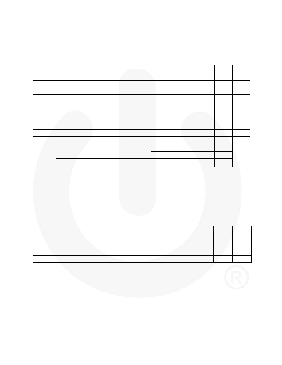
Absolute Maximum Ratings
Stresses exceeding the absolute maximum ratings may damage the device. The device may not function or be
operable above the recommended operating conditions and stressing the parts to these levels is not recommended.
In addition, extended exposure to stresses above the recommended operating conditions may affect device reliability.
The absolute maximum ratings are stress ratings only.
Symbol
Parameter
Min.
Max.
Units
VCC
Supply Voltage
-0.5
4.6
V
/OE
Output Enable Control Signal
-0.5
4.6
V
VSW
Switch I/O Voltage
(1)
VCC–4.6
4.6
V
IIK
Input Clamp Diode Current
- 50
mA
ISW
Switch I/O Current (Continuous)
100
mA
ISWPEAK
Peak Switch Current (Pulsed at 1ms Duration, <10% Duty Cycle)
150
mA
TSTG
Storage Temperature Range
-65
+150
°C
TJ
Maximum Junction Temperature
+150
°C
TL
Lead Temperature (Soldering, 10 seconds)
+260
°C
I/O to GND
12
All Other Pins
2
Human Body Model, JEDEC: JESD22-A114
VCC to GND
12
ESD
Charged Discharge Model, JEDEC: JESD22-C101
2
kV
Note
:
1. The input and output negative ratings may be exceeded if the input and output diode current ratings are observed.
Recommended Operating Conditions
The Recommended Operating Conditions table defines the conditions for actual device operation. Recommended
operating conditions are specified to ensure optimal performance to the datasheet specifications. Fairchild does not
recommend exceeding them or designing to Absolute Maximum Ratings.
Symbol
Parameter
Min.
Max.
Units
VCC
Supply Voltage
2.7
4.3
V
/OE
Output Enable Control Signal
3.0
4.3
V
VSW
Switch I/O Voltage
VCC -4.3
4.3
V
TA
Operating Temperature
-40
+85
°C
相关PDF资料 |
PDF描述 |
|---|---|
| FSA2156P6 | IC SWITCH SPST SC70-6 |
| FSA223MUX | MUX DPDT AUDIO/USB2.0 10MSOP |
| FSA2257MTCX | IC SWITCH DUAL SPDT 14TSSOP |
| FSA2258L10X | IC SWITCH DUAL SPDT 10MICROPAK |
| FSA2259UMX | IC SWITCH DUAL SPDT 10UMLP |
相关代理商/技术参数 |
参数描述 |
|---|---|
| FSA2156 | 制造商:FAIRCHILD 制造商全称:Fairchild Semiconductor 功能描述:Low-Voltage SPST 0.4ヘ Analog Switch |
| FSA2156_07 | 制造商:FAIRCHILD 制造商全称:Fairchild Semiconductor 功能描述:Low-Voltage SPST 0.4ヘ Analog Switch |
| FSA2156_11 | 制造商:FAIRCHILD 制造商全称:Fairchild Semiconductor 功能描述:Low-Voltage SPST 0.4?? Analog Switch |
| FSA2156FHX | 制造商:FAIRCHILD 制造商全称:Fairchild Semiconductor 功能描述:Low-Voltage SPST 0.4?? Analog Switch |
| FSA2156L6X | 功能描述:多路器开关 IC ANALOG_SWITCHES RoHS:否 制造商:Texas Instruments 通道数量:1 开关数量:4 开启电阻(最大值):7 Ohms 开启时间(最大值): 关闭时间(最大值): 传播延迟时间:0.25 ns 工作电源电压:2.3 V to 3.6 V 工作电源电流: 最大工作温度:+ 85 C 安装风格:SMD/SMT 封装 / 箱体:UQFN-16 |
发布紧急采购,3分钟左右您将得到回复。