- 您现在的位置:买卖IC网 > PDF目录1921 > FSA3200UMX (Fairchild Semiconductor)IC ANALOG USB VID SWITCH 16UMLP PDF资料下载
参数资料
| 型号: | FSA3200UMX |
| 厂商: | Fairchild Semiconductor |
| 文件页数: | 6/13页 |
| 文件大小: | 0K |
| 描述: | IC ANALOG USB VID SWITCH 16UMLP |
| 标准包装: | 5,000 |
| 功能: | USB 开关 |
| 电路: | 2 x DPST,2 x SPDT |
| 导通状态电阻: | 6.5 欧姆 |
| 电压电源: | 单电源 |
| 电压 - 电源,单路/双路(±): | 2.7 V ~ 4.5 V |
| 工作温度: | -40°C ~ 85°C |
| 安装类型: | 表面贴装 |
| 封装/外壳: | 16-UFQFN |
| 供应商设备封装: | 16-UMLP(1.8x2.6) |
| 包装: | 带卷 (TR) |
2010 Fairchild Semiconductor Corporation
www.fairchildsemi.com
FSA3200 Rev. 1.0.8
2
FSA3200
—
Two-Port,
High-Speed
USB2.0
Switch
with
Mobile
High-De
finition
Link
(MHL)
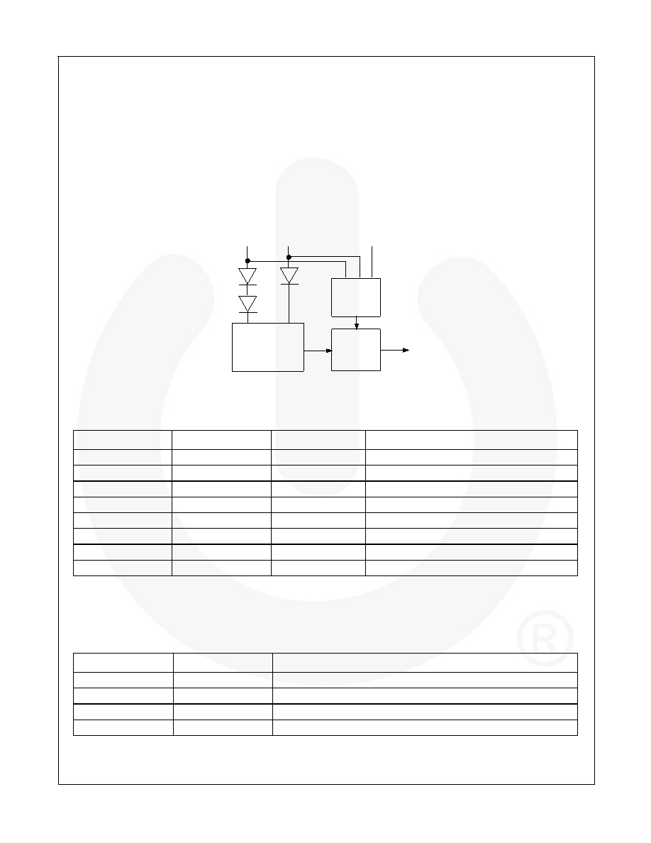
Switch Power Operation
In normal operation, the FSA3200 is powered from the
VCC pin, which typically is derived from a regulated
power management device. In special circumstances,
such as production test or system firmware upgrade, the
device can be powered from the VBUS pin. In this mode
of operation, a valid VBUS voltage is present (per USB2.0
specification) and VCC=0 V, typically due to a no-battery
condition. With the SELn pins strapped LOW (via
external resistor), the FSA3200 closes the USB path,
enabling the initial programming of the system directly
from the USB connector. Once the system has normal
operating supply power with VCC present, the VBUS
supply is not utilized and normal switch operation
commences. Optionally, the Power Select Override
(PSO) pin can be set HIGH to force the device to be
powered from VBUS.
The VBUS / VCC detection capability is not intended to be
an accurate determination of the voltages present,
rather a state condition detection to determine which
supply should be used. These state determinations rely
on the voltage conditions as described in the Electrical
Characterization tables below.
Figure 2. Simplified Logic of Switch Power Selection Circuit
Table 1. Switch Power Selection Truth Table
VCC
VBUS
PSO
(1)
Switch Power Source
0
No switch power, switch paths high-Z
0
1
0
VBUS
1
0
VCC
1
0
VCC
0
1
No switch power, switch paths high-Z
0
1
VBUS
1
0
1
VCC
(2)
1
VBUS
Notes:
1.
Control inputs should never be left floating or unconnected. If the PSO function is used, a weak pull-up resistor
(3 M) should be used to minimize static current draw. If the PSO function is not used, tie directly to GND.
2.
PSO control is overridden with no VBUS and the power selection is switched to VCC.
Table 2. Data Switch Select Truth Table
SEL1
(3)
SEL2
(3)
Function
0
D+/D- connected to USB+/USB-, IDCO connected to IDUSB
0
1
D+/D- connected to USB+/USB-, IDCOM connected to IDMDV
1
0
D+/D- connected to MDV+/MDV-, IDCOM connected to IDUSB
1
D+/D- connected to MDV+/MDV-, IDCOM connected to IDMDV
Note:
3.
Control inputs should never be left floating or unconnected. To guarantee default switch closure to the USB
position, the SEL pins should be tied to GND with a weak pull- down resistor (3 M) to minimize static current draw.
PSO
VCC
VBUS
Switch
Power
Charge Pump
& Regulator
Switch
Power
Selection
Switch
Power
Source
相关PDF资料 |
PDF描述 |
|---|---|
| FSA321UMX | IC SWITCH MULTIMEDIA 10-UMLP |
| FSA3259BQX | IC SWITCH DUAL SP3T 16DQFN |
| FSA3357K8X | IC SWITCH SP3T US8 |
| FSA4157AL6X_F087 | IC SWITCH SPDT 6MICROPAK |
| FSA4159L6X_F113 | IC SWITCH SPDT 6MICROPAK |
相关代理商/技术参数 |
参数描述 |
|---|---|
| FSA3200UMX_F106 | 功能描述:电源开关 IC - USB USB SW DPDT 5V RoHS:否 制造商:Micrel 电源电压-最小:2.7 V 电源电压-最大:5.5 V 最大工作温度:+ 85 C 最小工作温度:- 40 C 封装 / 箱体:SOIC-8 封装:Tube |
| FSA321 | 制造商:FAIRCHILD 制造商全称:Fairchild Semiconductor 功能描述:USB2.0 Hi-Speed (480Mbps) and Audio Switches with Negative Signal Capability and Built-in Termination on Unselected Audio Paths |
| FSA321_12 | 制造商:FAIRCHILD 制造商全称:Fairchild Semiconductor 功能描述:USB2.0 Hi-Speed (480Mbps) and Audio Switches with Negative Signal Capability and Built-in Termination on Unselected Audio Paths |
| FSA321UMX | 功能描述:多路器开关 IC USB 2.0 Hi-Speed and Audio Switch RoHS:否 制造商:Texas Instruments 通道数量:1 开关数量:4 开启电阻(最大值):7 Ohms 开启时间(最大值): 关闭时间(最大值): 传播延迟时间:0.25 ns 工作电源电压:2.3 V to 3.6 V 工作电源电流: 最大工作温度:+ 85 C 安装风格:SMD/SMT 封装 / 箱体:UQFN-16 |
| FSA321UMX_F113 | 功能描述:多路器开关 IC Multimedia & USB2 Hi-Speed & Aud Swtch RoHS:否 制造商:Texas Instruments 通道数量:1 开关数量:4 开启电阻(最大值):7 Ohms 开启时间(最大值): 关闭时间(最大值): 传播延迟时间:0.25 ns 工作电源电压:2.3 V to 3.6 V 工作电源电流: 最大工作温度:+ 85 C 安装风格:SMD/SMT 封装 / 箱体:UQFN-16 |
发布紧急采购,3分钟左右您将得到回复。