- 您现在的位置:买卖IC网 > PDF目录68995 > FSCM0565RCYDTU_NL (FAIRCHILD SEMICONDUCTOR CORP) 20 A SWITCHING REGULATOR, 72 kHz SWITCHING FREQ-MAX, PZFM6 PDF资料下载
参数资料
| 型号: | FSCM0565RCYDTU_NL |
| 厂商: | FAIRCHILD SEMICONDUCTOR CORP |
| 元件分类: | 稳压器 |
| 英文描述: | 20 A SWITCHING REGULATOR, 72 kHz SWITCHING FREQ-MAX, PZFM6 |
| 封装: | TO-220, 6PIN |
| 文件页数: | 2/23页 |
| 文件大小: | 604K |
| 代理商: | FSCM0565RCYDTU_NL |
FSCM0565R
10
Functional Description
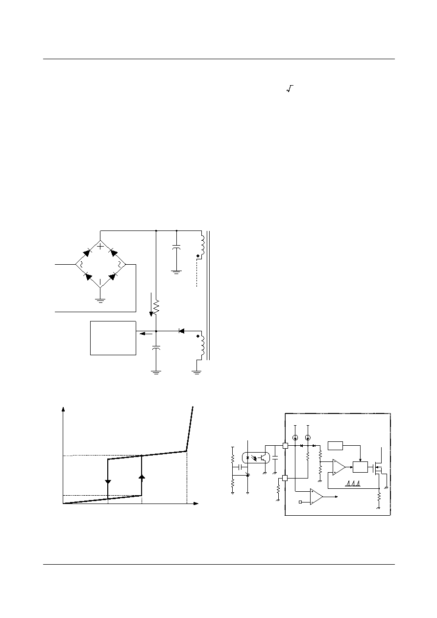
1. Startup: Figure 16 shows the typical startup circuit and
transformer
auxiliary
winding
for
the
FSCM0565R
application. Before the FSCM0565R begins switching, it
consumes only startup current (typically 25uA) and the
current supplied from the DC link supply current consumed
by the FPS (Icc), and charges the external capacitor (Ca) that
is connected to the Vcc pin. When Vcc reaches start voltage
of 12V (VSTART), the FSCM0565R begins switching, and the
current consumed by the FSCM0565R increases to 3mA.
Then, the FSCM0565R continues its normal switching
operation and the power required for this device is supplied
from the transformer auxiliary winding, unless Vcc drops
below the stop voltage of 8V (VSTOP). To guarantee the
stable operation of the control IC, Vcc has under voltage
lockout (UVLO) with 4V hysteresis. Figure 17 shows the
relation between the current consumed by the FPS (ICC) and
the supply voltage (VCC)
Figure 16. Startup Circuit
Figure 17. Relation Between O
perating Supply Current
and Vcc Voltage
The minimum current supplied through the startup resistor is
given by
where Vline
min is the minimum input voltage, Vstart is the
start voltage (12V) and Rstr is the startup resistor. The startup
resistor should be chosen so that Isup
min is larger than the
maximum startup current (40uA). If not, VCC can not be
charged to the start voltage and FPS will fail to start up.
2. Feedback Control: The FSCM0565R employs current
mode control, as shown in Figure 18. An opto-coupler (such
as the H11A817A) and a shunt regulator (such as the
KA431) are typically used to implement the feedback
network. Comparing the feedback voltage with the voltage
across the Rsense resistor makes it possible to control the
switching duty cycle. When the reference pin voltage of the
KA431 exceeds the internal reference voltage of 2.5V, the
H11A817A LED current increases, thus pulling down the
feedback voltage and reducing the duty cycle. This event
typically happens when the input voltage is increased or the
output load is decreased.
2.1 Pulse-by-pulse Current Limit: Because current mode
control is employed, the peak current through the SenseFET
is determined by the inverting input of the PWM comparator
(Vfb*) as shown in Figure 18. When the current through the
opto transistor is zero and the current limit pin (#5) is left
floating, the feedback current source (IFB) of 0.9mA flows
only through the internal resistor (R+2.5R=2.8k). In this
case, the cathode voltage of diode D2 and the peak drain
current have maximum values of 2.5V and 2.5A, respec-
tively. The pulse-by-pulse current limit can be adjusted using
a resistor to GND on the current limit pin (#5). The current
limit level using an external resistor (RLIM) is given by
Figure 18. Pulse Width Modulation (PWM) Circuit
2.2 Leading Edge Blanking (LEB): At the instant the
internal SenseFET is turned on, there usually exists a high
FSCM 0565R
Rstr
V
CC
Ca
Da
I
SUP
AC line
(V
line
min
- V
line
max )
C
DC
I
CC
I
CC
V
CC
Vstop=8V
25uA
3mA
Vstart=12V
Vz
Power Up
Power Down
I
sup
min
2V
line
min
V
start
–
()
1
R
str
------------
=
I
LIM
R
LIM
2.5A
2.8k
Ω R
LIM
+
------------------------------------
=
4
OSC
Vcc
Vref
I
delay
I
FB
V
SD
R
2.5R
Gate
driver
OLP
D1
D2
+
V
fb*
-
Vfb
KA431
C
B
Vo
H11A817A
R
sense
SenseFET
6
R
LI M
0.9mA
0.3k
相关PDF资料 |
PDF描述 |
|---|---|
| FSCM0765RCYDTU_NL | 21 A SWITCHING REGULATOR, 72 kHz SWITCHING FREQ-MAX, PSFM6 |
| FSCT11A-UH5 | BRUSHLESS DC MOTOR CONTROLLER, PSIP5 |
| FSCT07A-UH5 | BRUSHLESS DC MOTOR CONTROLLER, PSIP5 |
| FSCT17A-UH5 | BRUSHLESS DC MOTOR CONTROLLER, PSIP5 |
| FSD210_NL | 0.365 A SWITCHING REGULATOR, 142 kHz SWITCHING FREQ-MAX, PDIP7 |
相关代理商/技术参数 |
参数描述 |
|---|---|
| FSCM0565RD | 制造商:Fairchild Semiconductor Corporation 功能描述:POWER SWITCH SMPS GREEN D2-PAK-5 |
| FSCM0565RG | 制造商:FAIRCHILD 制造商全称:Fairchild Semiconductor 功能描述:Green Mode Fairchild Power Switch |
| FSCM0565RGTU | 功能描述:IC SWIT PWM GREEN CM HV TO220 RoHS:是 类别:集成电路 (IC) >> PMIC - AC-DC 转换器,离线开关 系列:- 标准包装:1 系列:FPS™ 输出隔离:隔离 频率范围:61kHz ~ 73kHz 输入电压:8 V ~ 26 V 输出电压:650V 功率(瓦特):12W 工作温度:-40°C ~ 115°C 封装/外壳:8-DIP(0.300",7.62mm) 供应商设备封装:8-MDIP 包装:Digi-Reel® 其它名称:FSL206MRBNFSDKR |
| FSCM0565RGWDTU | 功能描述:电源开关 IC - 配电 FPS FOR LCD RoHS:否 制造商:Exar 输出端数量:1 开启电阻(最大值):85 mOhms 开启时间(最大值):400 us 关闭时间(最大值):20 us 工作电源电压:3.2 V to 6.5 V 电源电流(最大值): 最大工作温度:+ 85 C 安装风格:SMD/SMT 封装 / 箱体:SOT-23-5 |
| FSCM0565RI | 制造商:FAIRCHILD 制造商全称:Fairchild Semiconductor 功能描述:Green Mode Fairchild Power Switch (FPS) |
发布紧急采购,3分钟左右您将得到回复。