- 您现在的位置:买卖IC网 > PDF目录68995 > FSDL312 (FAIRCHILD SEMICONDUCTOR CORP) 4 A SWITCHING REGULATOR, PDIP8 PDF资料下载
参数资料
| 型号: | FSDL312 |
| 厂商: | FAIRCHILD SEMICONDUCTOR CORP |
| 元件分类: | 稳压器 |
| 英文描述: | 4 A SWITCHING REGULATOR, PDIP8 |
| 封装: | DIP-8 |
| 文件页数: | 2/16页 |
| 文件大小: | 607K |
| 代理商: | FSDL312 |
FSDL312
10
Functional Description
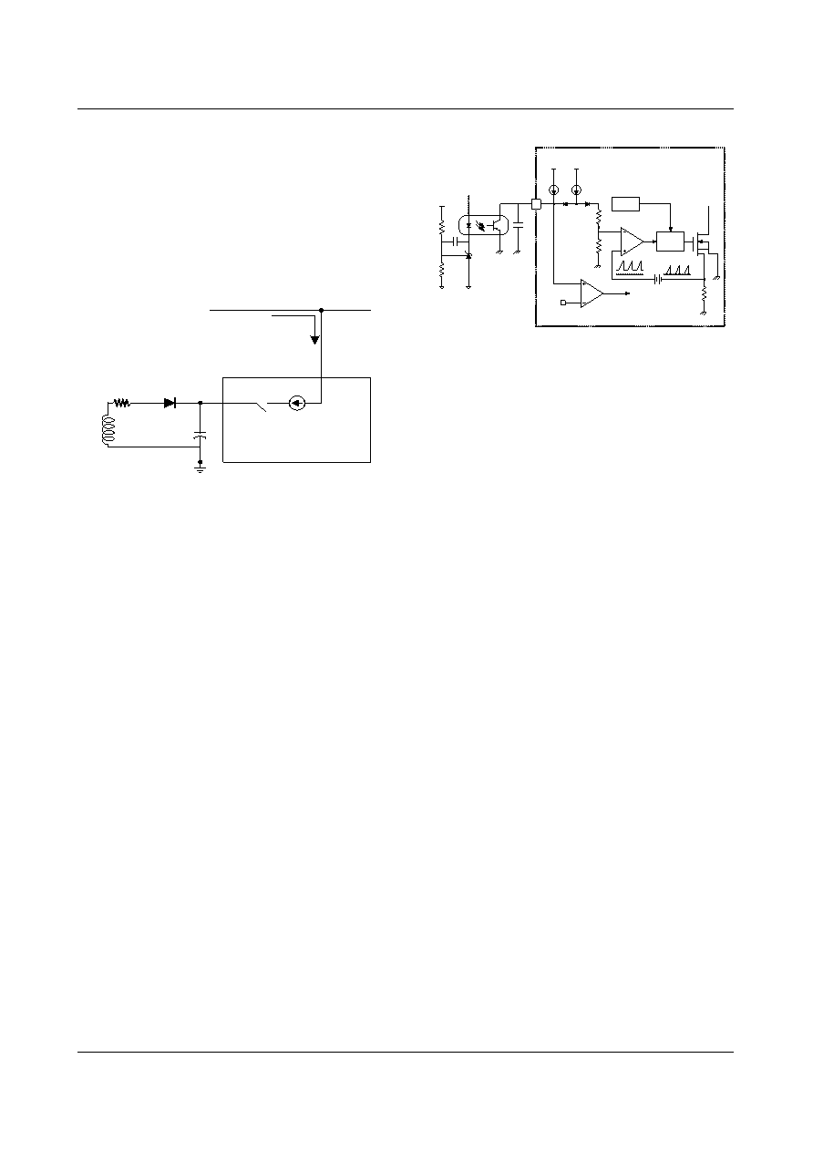
1. Startup : In previous generations of Fairchild Power
Switches (FPSTM) the Vstr pin had an external resistor to the
DC input voltage line. In this generation the startup resistor
is replaced by an internal high voltage current source and a
switch that shuts off when 15mS goes by after the supply
voltage, Vcc, gets above 12V. The source turns back on if
Vcc drops below 8V.
Figure 4. High voltage current source
2. Feedback Control : The FSDL312 employs current mode
control, shown in figure 5. An opto-coupler (such as the
H11A817A) and shunt regulator (such as the KA431) are
typically used to implement the feedback network. Compar-
ing the feedback voltage with the voltage across the Rsense
resistor plus an offset voltage makes it possible to control the
switching duty cycle. When the reference pin voltage of the
KA431 exceeds the internal reference voltage of 2.5V, the
H11A817A LED current increases, thus pulling down the
feedback voltage and reducing the duty cycle. This event
typically happens when the input voltage is increased or the
output load is decreased.
3. Leading edge blanking (LEB) : At the instant the internal
Sense FET is turned on, there usually exists a high current
spike through the Sense FET, caused by the primary side
capacitance and secondary side rectifier diode reverse recov-
ery. Excessive voltage across the Rsense resistor would lead
to incorrect feedback operation in the current mode PWM
control. To counter this effect, the FPSTM employs a leading
edge blanking (LEB) circuit. This circuit inhibits the PWM
comparator for a short time (TLEB) after the Sense FET is
turned on.
Figure 5. Pulse width modulation (PWM) circuit
4. Protection Circuit : The FPSTM has several protective func-
tions such as over load protection (OLP), over voltage pro-
tection (OVP), abnormal over current protection (AOCP),
under voltage lock out (UVLO) and thermal shutdown
(TSD). Because these protection circuits are fully integrated
inside the IC without external components, the reliability is
improved without increasing cost. Once the fault condition
occurs, switching is terminated and the Sense FET remains
off. This causes Vcc to fall. When Vcc reaches the UVLO
stop voltage, 8V, the protection is reset and the internal high
voltage current source charges the Vcc capacitor via the Vstr
pin. When Vcc reaches the UVLO start voltage,12V, the
FPSTM resumes its normal operation. In this manner, the
auto-restart can alternately enable and disable the switching
of the power Sense FET until the fault condition is elimi-
nated.
4.1 Over Load Protection (OLP) : Overload is defined as the
load current exceeding a pre-set level due to an unexpected
event. In this situation, the protection circuit should be acti-
vated in order to protect the SMPS. However, even when the
SMPS is in the normal operation, the over load protection
circuit can be activated during the load transition. In order to
avoid this undesired operation, the over load protection cir-
cuit is designed to be activated after a specified time to deter-
mine whether it is a transient situation or an overload
situation. In conjunction with the Ipk current limit pin (if
used) the current mode feedback path would limit the current
in the Sense FET when the maximum PWM duty cycle is
attained. If the output consumes more than this maximum
power, the output voltage (Vo) decreases below the set volt-
age. This reduces the current through the opto-coupler LED,
which also reduces the opto-coupler transistor current, thus
increasing the feedback voltage (Vfb). If Vfb exceeds 3V, the feed-
back input diode is blocked and the 5uA Idelay current source starts
to charge Cfb slowly up to Vcc. In this condition, Vfb continues
increasing until it reaches 6V, when the switching operation is ter-
minated as shown in figure 6. The delay time for shutdown is the
time required to charge Cfb from 3V to 6V with 5uA.
Vin,dc
Vstr
Vcc
15m S After UVLO
start(>12V)
off
UVLO <8V
on
Istr
J-FET
3
OSC
Vcc
Vref
2uA
0.9mA
V
SD
R
28R
FB
Gate
driver
OLP
D1
D2
Vfb*
Vfb
431
Cfb
Vo
相关PDF资料 |
PDF描述 |
|---|---|
| FSEZ1317AMY-F116 | SWITCHING CONTROLLER, 53 kHz SWITCHING FREQ-MAX, PDSO7 |
| FSGM0465RWDTU | SWITCHING CONTROLLER, ZFM6 |
| FSL106MR | 0.62 A SWITCHING CONTROLLER, 73 kHz SWITCHING FREQ-MAX, PDIP8 |
| FSL116HR | 1.24 A SWITCHING CONTROLLER, 110 kHz SWITCHING FREQ-MAX, DIP8 |
| FSL126HR | 1.68 A SWITCHING CONTROLLER, 110 kHz SWITCHING FREQ-MAX, PDIP8 |
相关代理商/技术参数 |
参数描述 |
|---|---|
| FSDL321 | 功能描述:电源开关 IC - 配电 FPS for DVDP/STB RoHS:否 制造商:Exar 输出端数量:1 开启电阻(最大值):85 mOhms 开启时间(最大值):400 us 关闭时间(最大值):20 us 工作电源电压:3.2 V to 6.5 V 电源电流(最大值): 最大工作温度:+ 85 C 安装风格:SMD/SMT 封装 / 箱体:SOT-23-5 |
| FSDL321L | 功能描述:电源开关 IC - 配电 FPS for DVDP/STB RoHS:否 制造商:Exar 输出端数量:1 开启电阻(最大值):85 mOhms 开启时间(最大值):400 us 关闭时间(最大值):20 us 工作电源电压:3.2 V to 6.5 V 电源电流(最大值): 最大工作温度:+ 85 C 安装风格:SMD/SMT 封装 / 箱体:SOT-23-5 |
| FSDL321L_Q | 功能描述:电源开关 IC - 配电 FPS for DVDP/STB RoHS:否 制造商:Exar 输出端数量:1 开启电阻(最大值):85 mOhms 开启时间(最大值):400 us 关闭时间(最大值):20 us 工作电源电压:3.2 V to 6.5 V 电源电流(最大值): 最大工作温度:+ 85 C 安装风格:SMD/SMT 封装 / 箱体:SOT-23-5 |
| FSDLC01G-S | 制造商:AXIOMTEK 制造商全称:AXIOMTEK 功能描述:Capacity: 128MB to 32GB |
| FSDLC128-S | 制造商:AXIOMTEK 制造商全称:AXIOMTEK 功能描述:Capacity: 128MB to 32GB |
发布紧急采购,3分钟左右您将得到回复。