- 您现在的位置:买卖IC网 > PDF目录68995 > FSEZ1317AMY-F116 (FAIRCHILD SEMICONDUCTOR CORP) SWITCHING CONTROLLER, 53 kHz SWITCHING FREQ-MAX, PDSO7 PDF资料下载
参数资料
| 型号: | FSEZ1317AMY-F116 |
| 厂商: | FAIRCHILD SEMICONDUCTOR CORP |
| 元件分类: | 稳压器 |
| 英文描述: | SWITCHING CONTROLLER, 53 kHz SWITCHING FREQ-MAX, PDSO7 |
| 封装: | GREEN, MS-012AA, SOP-8/7 |
| 文件页数: | 4/16页 |
| 文件大小: | 1031K |
| 代理商: | FSEZ1317AMY-F116 |
2010 Fairchild Semiconductor Corporation
www.fairchildsemi.com
FSEZ1317A Rev. 1.0.1
12
FSEZ1317A
—
Prima
ry-Side-Regulation
PWM
with
P
O
WER
MOSFET
Integrated
Under-Voltage Lockout (UVLO)
The turn-on and turn-off thresholds are fixed internally at
16V and 5V, respectively. During startup, the hold-up
capacitor must be charged to 16V through the startup
resistor to enable the FSEZ1317A. The hold-up
capacitor continues to supply VDD until power can be
delivered from the auxiliary winding of the main
transformer. VDD is not allowed to drop below 5V during
this startup process. This UVLO hysteresis window
ensures that hold-up capacitor properly supplies VDD
during startup.
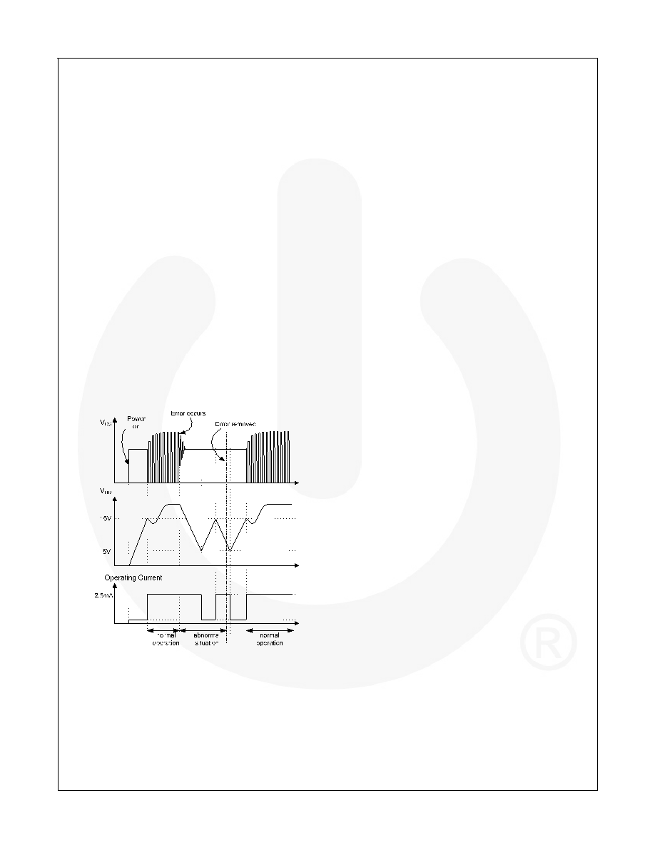
Protections
The FSEZ1317A has several self-protection functions,
such
as
Over-Voltage
Protection
(OVP),
Over-
Temperature Protection (OTP), and pulse-by-pulse
current limit. All the protections are implemented as
auto-restart mode. Once the abnormal condition occurs,
the switching is terminated and the MOSFET remains
off, causing VDD to drop. When VDD drops to the VDD
turn-off voltage of 5V, internal startup circuit is enabled
again and the supply current drawn from the HV pin
charges the hold-up capacitor. When VDD reaches the
turn-on voltage of 16V, normal operation resumes. In
this manner, the auto-restart alternately enables and
disables the switching of the MOSFET until the
abnormal condition is eliminated (see Figure 29).
Figure 29. Auto-Restart Operation
VDD Over-Voltage Protection (OVP)
VDD over-voltage protection prevents damage from over-
voltage conditions. If the VDD voltage exceeds 24V at
open-loop feedback condition, OVP is triggered and the
PWM switching is disabled. The OVP has a debounce
time (typically 200s) to prevent false triggering due to
switching noises.
Over-Temperature Protection (OTP)
The built-in temperature-sensing circuit shuts down
PWM output if the junction temperature exceeds 140°C.
Pulse-by-pulse Current Limit
When the sensing voltage across the current-sense
resistor exceeds the internal threshold of 0.8V, the
MOSFET is turned off for the remainder of switching
cycle. In normal operation, the pulse-by-pulse current
limit is not triggered since the peak current is limited by
the control loop.
Leading-Edge Blanking (LEB)
Each time the power MOSFET switches on, a turn-on
spike occurs at the sense resistor. To avoid premature
termination of the switching pulse, a leading-edge
blanking time is built in. During this blanking period,
the current-limit comparator is disabled and cannot
switch off the gate driver. As a result conventional RC
filtering can be omitted.
Gate Output
The FSEZ1317A output stage is a fast totem-pole gate
driver. Cross conduction has been avoided to minimize
heat dissipation, increase efficiency, and enhance
reliability. The output driver is clamped by an internal
15V Zener diode to protect the power MOSFET
transistors against undesired over-voltage gate signals.
Built-In Slope Compensation
The sensed voltage across the current-sense resistor is
used for current mode control and pulse-by-pulse
current limiting. Built-in slope compensation improves
stability and prevents sub-harmonic oscillations due to
peak-current mode control. The FSEZ1317A has a
synchronized, positive-slope ramp built-in at each
switching cycle.
Noise Immunity
Noise from the current sense or the control signal can
cause significant pulsewidth jitter, particularly in
continuous-conduction
mode.
While
slope
compensation helps alleviate these problems, further
precautions should still be taken. Good placement and
layout practices should be followed. Avoiding long PCB
traces and component leads, locating compensation
and filter components near the FSEZ1317A, and
increasing the power MOS gate resistance are advised.
相关PDF资料 |
PDF描述 |
|---|---|
| FSGM0465RWDTU | SWITCHING CONTROLLER, ZFM6 |
| FSL106MR | 0.62 A SWITCHING CONTROLLER, 73 kHz SWITCHING FREQ-MAX, PDIP8 |
| FSL116HR | 1.24 A SWITCHING CONTROLLER, 110 kHz SWITCHING FREQ-MAX, DIP8 |
| FSL126HR | 1.68 A SWITCHING CONTROLLER, 110 kHz SWITCHING FREQ-MAX, PDIP8 |
| FSL126MR | 8 A SWITCHING CONTROLLER, 73 kHz SWITCHING FREQ-MAX, PDIP8 |
相关代理商/技术参数 |
参数描述 |
|---|---|
| FSEZ1317MY | 功能描述:初级与次级侧 PWM 控制器 EZSWITCH PSR PWM Cont. w/ Int. MOSFET RoHS:否 制造商:ON Semiconductor 输出端数量:1 开关频率:250 KHz 工作电源电压:- 0.3 V to + 28 V 最大工作温度:+ 85 C 最小工作温度:- 5 C 封装 / 箱体:SOIC-8 Narrow 封装:Reel |
| FSEZ1317NY | 功能描述:初级与次级侧 PWM 控制器 EZSWITCH PSR PWM Cont. w/ Int. MOSFET RoHS:否 制造商:ON Semiconductor 输出端数量:1 开关频率:250 KHz 工作电源电压:- 0.3 V to + 28 V 最大工作温度:+ 85 C 最小工作温度:- 5 C 封装 / 箱体:SOIC-8 Narrow 封装:Reel |
| FSEZ1317WAMY | 功能描述:初级与次级侧 PWM 控制器 PSR PWM Controller w/MOSFET RoHS:否 制造商:ON Semiconductor 输出端数量:1 开关频率:250 KHz 工作电源电压:- 0.3 V to + 28 V 最大工作温度:+ 85 C 最小工作温度:- 5 C 封装 / 箱体:SOIC-8 Narrow 封装:Reel |
| FSEZ13X7 | 制造商:FAIRCHILD 制造商全称:Fairchild Semiconductor 功能描述:Primary Side Regulated (PSR) Flyback Converter |
| FSEZ2007NY | 功能描述:电压模式 PWM 控制器 Low-Power Green-Mode EZSWITCH RoHS:否 制造商:Texas Instruments 输出端数量:1 拓扑结构:Buck 输出电压:34 V 输出电流: 开关频率: 工作电源电压:4.5 V to 5.5 V 电源电流:600 uA 最大工作温度:+ 125 C 最小工作温度:- 40 C 封装 / 箱体:WSON-8 封装:Reel |
发布紧急采购,3分钟左右您将得到回复。