- 您现在的位置:买卖IC网 > PDF目录19696 > FSQ321 (Fairchild Semiconductor)IC SWIT PWM GREEN OVP UVLO 8DIP PDF资料下载
参数资料
| 型号: | FSQ321 |
| 厂商: | Fairchild Semiconductor |
| 文件页数: | 12/21页 |
| 文件大小: | 0K |
| 描述: | IC SWIT PWM GREEN OVP UVLO 8DIP |
| 标准包装: | 50 |
| 输出隔离: | 隔离 |
| 频率范围: | 55kHz ~ 67kHz |
| 输入电压: | 9 V ~ 20 V |
| 输出电压: | 650V |
| 功率(瓦特): | 12W |
| 工作温度: | -40°C ~ 85°C |
| 封装/外壳: | 8-DIP(0.300",7.62mm) |
| 供应商设备封装: | 8-DIP |
| 包装: | 管件 |
| 产品目录页面: | 1219 (CN2011-ZH PDF) |
�� �
�
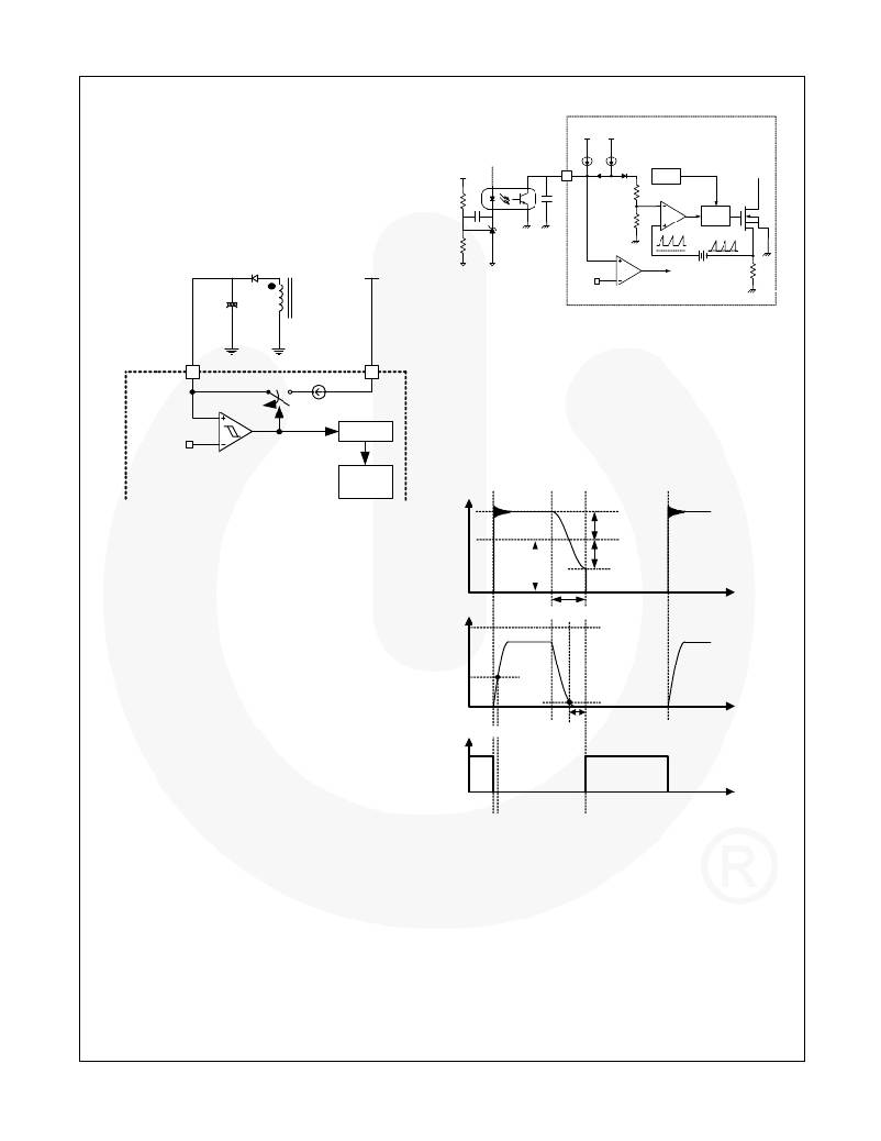
�Functional� Description�
�1.� Startup� :� At� startup,� an� internal� high-voltage� current�
�source� supplies� the� internal� bias� and� charges� the�
�external� capacitor� (C� a� )� connected� to� the� V� CC� pin,� as�
�illustrated� in� Figure� 20.� When� V� CC� reaches� 12V,� the�
�FPS?� begins� switching� and� the� internal� high-voltage�
�current� source� is� disabled.� The� FPS� continues� its�
�V� O�
�FOD817A�
�V� FB�
�C� B�
�3�
�V� CC�
�I� delay�
�D1�
�V� ref�
�I� FB�
�D2�
�3R�
�OSC�
�SenseFET�
�normal� switching� operation� and� the� power� is� supplied�
�from� the� auxiliary� transformer� winding� unless� V� CC� goes�
�below� the� stop� voltage� of� 8V.�
�V� DC�
�KA431�
�V� SD�
�+�
�V� FB� *�
�-�
�R�
�OLP�
�Gate�
�driver�
�R� sense�
�FSQ0365RN� Rev.� 00�
�C� a�
�Figure� 21.� Pulse-Width-Modulation� (PWM)� Circuit�
�2�
�V� CC�
�5�
�V� str�
�3.� Synchronization� :� The� FSQ-series� employs� a� valley�
�switching� technique� to� minimize� the� switching� noise� and�
�loss.� The� basic� waveforms� of� the� valley� switching�
�I� CH�
�converter� are� shown� in� Figure� 22.� To� minimize� the�
�MOSFET's� switching� loss,� the� MOSFET� should� be�
�8V/12V�
�FSQ0365RN� Rev.00�
�V� CC� good�
�V� ref�
�Internal�
�Bias�
�turned� on� when� the� drain� voltage� reaches� its� minimum�
�value,� as� shown� in� Figure� 22.� The� minimum� drain�
�voltage� is� indirectly� detected� by� monitoring� the� V� CC�
�winding� voltage,� as� shown� in� Figure� 22.�
�V� ds�
�Figure� 20.� Startup� Circuit�
�2.� Feedback� Control� :� FPS� employs� Current� Mode�
�V� RO�
�control,� as� shown� in� Figure� 21.� An� opto-coupler� (such� as�
�FOD817A)� and� shunt� regulator� (such� as� KA431)� are�
�often� used� to� implement�
�the� feedback� network.�
�V� DC�
�V� RO�
�Comparing� the� feedback� voltage� with� the� voltage� across�
�the� R� SENSE� resistor� makes� it� possible� to� control� the�
�switching� duty� cycle.� When� the� reference� pin� voltage� of�
�V� sync�
�t� F�
�V� ovp� (6V)�
�the� shunt� regulator� exceeds� the� internal� reference�
�voltage� of� 2.5V,� the� opto-coupler� LED� current� increases,�
�pulling� down� the� feedback� voltage� and� reducing� the� duty�
�cycle.� This� event� typically� occurs� when� input� voltage� is�
�increased� or� output� load� is� decreased.�
�2.1� Pulse-by-Pulse� Current� Limit� :� Because� Current�
�Mode� control� is� employed,� the� peak� current� through� the�
�SenseFET� is� limited� by� the� inverting� input� of� PWM�
�MOSFET� Gate�
�0.7V�
�0.2V�
�300ns� Delay�
�comparator� (V� FB� *),� as� shown� in� Figure� 21.� Assuming�
�that� the� 0.9mA� current� source� flows� only� through� the�
�ON�
�ON�
�internal� resistor� (3R� +� R� =� 2.8k� ?� ),� the� cathode� voltage�
�of� diode� D2� is� about� 2.5V.� Since� D1� is� blocked� when� the�
�feedback� voltage� (V� FB� )� exceeds� 2.5V,� the� maximum�
�voltage� of� the� cathode� of� D2� is� clamped� at� this� voltage,�
�clamping� V� FB� *.� Therefore,� the� peak� value� of� the� current�
�through� the� SenseFET� is� limited.�
�2.2� Leading-Edge� Blanking� (LEB)� :� At� the� instant� the�
�internal� SenseFET� is� turned� on,� a� high-current� spike�
�usually� occurs� through� the� SenseFET,� caused� by�
�primary-side� capacitance� and� secondary-side� rectifier�
�reverse� recovery.� Excessive� voltage� across� the� R� sense�
�resistor� would� lead� to� incorrect� feedback� operation� in� the�
�Current� Mode� PWM� control.� To� counter� this� effect,� the�
�FPS� employs� a� leading-edge� blanking� (LEB)� circuit.� This�
�circuit� inhibits� the� PWM� comparator� for� a� short� time�
�(t� LEB� )� after� the� SenseFET� is� turned� on.�
�?� 2007� Fairchild� Semiconductor� Corporation�
�FSQ0365,� FSQ0265,� FSQ0165,� FSQ321� ?� Rev.� 1.0.6�
�FSQ0365RN� Rev.00�
�Figure� 22.� Valley� Resonant� Switching� Waveforms�
�4.� Protection� Circuits� :� The� FSQ-series� has� several�
�self-protective� functions,� such� as� Overload� Protection�
�(OLP),� Abnormal� Over-Current� protection� (AOCP),�
�Over-Voltage� Protection� (OVP),� and� Thermal� Shutdown�
�(TSD).� All� the� protections� are� implemented� as� Auto-�
�Restart� Mode.� Once� the� fault� condition� is� detected,�
�switching� is� terminated� and� the� SenseFET� remains� off.�
�This� causes� V� CC� to� fall.� When� V� CC� falls� down� to� the�
�Under-Voltage� Lockout� (UVLO)� stop� voltage� of� 8V,� the�
�protection� is� reset� and� the� startup� circuit� charges� the�
�V� CC� capacitor.� When� the� V� CC� reaches� the� start� voltage�
�of� 12V,� the� FSQ-series� resumes� normal� operation.� If� the�
�fault� condition� is� not� removed,� the� SenseFET� remains�
�off� and� V� CC� drops� to� stop� voltage� again.� In� this� manner,�
�www.fairchildsemi.com�
�12�
�相关PDF资料 |
PDF描述 |
|---|---|
| MIC5201-3.3BM | IC REG LDO 3.3V .2A 8-SOIC |
| AGM28DRSD-S288 | CONN EDGECARD EXTEND 56POS .156 |
| LC4256B-3FT256AC | IC PLD 256MC 128I/O 3NS 256FTBGA |
| MIC5202-4.8BM TR | IC REG LDO 4.85V .1A 8-SOIC |
| 190-025-263R001 | CONN DB25 FEMALE R/A SOLDER SMD |
相关代理商/技术参数 |
参数描述 |
|---|---|
| FSQ321L | 功能描述:开关变换器、稳压器与控制器 SMPS Power Switch RoHS:否 制造商:Texas Instruments 输出电压:1.2 V to 10 V 输出电流:300 mA 输出功率: 输入电压:3 V to 17 V 开关频率:1 MHz 工作温度范围: 安装风格:SMD/SMT 封装 / 箱体:WSON-8 封装:Reel |
| FSQ321LX | 功能描述:开关变换器、稳压器与控制器 0.5A, 650V SMPS Power Switch RoHS:否 制造商:Texas Instruments 输出电压:1.2 V to 10 V 输出电流:300 mA 输出功率: 输入电压:3 V to 17 V 开关频率:1 MHz 工作温度范围: 安装风格:SMD/SMT 封装 / 箱体:WSON-8 封装:Reel |
| FSQ3W | 制造商:RFE 制造商全称:RFE international 功能描述:FUSIBLE RESISTORS FM, FKN, & FSQ Series: Fusible |
| FSQ500HL | 功能描述:电源开关 IC - 配电 Green Mode Power Switch RoHS:否 制造商:Exar 输出端数量:1 开启电阻(最大值):85 mOhms 开启时间(最大值):400 us 关闭时间(最大值):20 us 工作电源电压:3.2 V to 6.5 V 电源电流(最大值): 最大工作温度:+ 85 C 安装风格:SMD/SMT 封装 / 箱体:SOT-23-5 |
| FSQ500L | 功能描述:电源开关 IC - 配电 Power Switch 0.245A RoHS:否 制造商:Exar 输出端数量:1 开启电阻(最大值):85 mOhms 开启时间(最大值):400 us 关闭时间(最大值):20 us 工作电源电压:3.2 V to 6.5 V 电源电流(最大值): 最大工作温度:+ 85 C 安装风格:SMD/SMT 封装 / 箱体:SOT-23-5 |
发布紧急采购,3分钟左右您将得到回复。