参数资料
| 型号: | FSUSB46UMX |
| 厂商: | Fairchild Semiconductor |
| 文件页数: | 7/12页 |
| 文件大小: | 0K |
| 描述: | IC USB SWITCH DPST 8UMLP |
| 标准包装: | 5,000 |
| 功能: | USB 开关 |
| 电路: | 1 x DPST - NC |
| 导通状态电阻: | 6.5 欧姆 |
| 电压电源: | 单电源 |
| 电压 - 电源,单路/双路(±): | 3 V ~ 4.3 V |
| 工作温度: | -40°C ~ 85°C |
| 安装类型: | 表面贴装 |
| 封装/外壳: | 8-UMLP |
| 供应商设备封装: | 8-UMLP |
| 包装: | 带卷 (TR) |
4
SY58040U
Micrel, Inc.
M9999-103009
hbwhelp@micrel.com or (408) 955-1690
AbsoluteMaximumRatings(1)
Power Supply Voltage (VCC ) .......................–0.5V to +4.0V
Input Voltage (VIN)...........................................–0.5V to VCC
CML Output Voltage (VOUT) ..........VCC –0.5V to VCC +5.0V
Termination Current(3)
Source or sink current on VT pin ........................ ±100mA
Input Current(3)
Source or sink current on IN, /IN .......................... ±50mA
VREF-AC Current(3)
Source or sink current on IN, /IN ............................ ±2mA
Lead Temperature (soldering, 20 sec.)...................... 260°C
Storage Temperature Range (TS )............ –65°C to +150°C
Operating Ratings(2)
Power Supply Voltage (VCC) ................. +2.375V to +3.60V
Ambient Temperature Range (TA) .............. –40°C to +85°C
Package Thermal Resistance(4)
QFN (θJA)
Still-Air ............................................................. 23°C/W
QFN (ψJB)
Junction-to-board............................................. 12°C/W
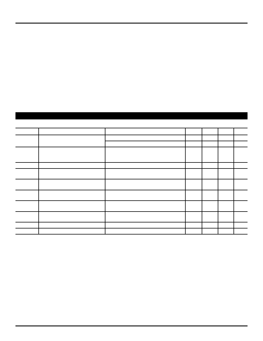
Symbol
Parameter
Condition
Min
Typ
Max
Units
VCC
Power Supply Voltage
VCC = 2.5V.
2.375
2.5
2.625
V
VCC = 3.3V.
3.0
3.3
3.6
V
ICC
Power Supply Current
No load, max. VCC.
225
300
mA
Includes current from internal 50 pull-up
on each output.
RIN
Input Resistance (IN-to-VT, /IN-to-VT)
45
50
55
RDIFF_IN
Differential Input Resistance
90
100
110
(IN-to-/IN)
VIH
Input HIGH Voltage
Note6
VCC–1.6
VCC
V
(IN-to-/IN)
VIL
Input LOW Voltage
0
VIH–0.1
V
(IN-to-/IN)
VIN
Input Voltage Swing
See Figure 1a.
0.1
1.7
V
(IN-to-/IN)
VDIFF_IN
Differential Input Voltage Swing
See Figure 1b.
0.2
V
|IN – /IN|
VT_IN
IN to VT (IN-to-/IN)
1.28
V
VREF-AC
Output Reference Voltage
VCC–1.3 VCC–1.2 VCC–1.1
V
Notes:
1. Permanent device damage may occur if ratings in the “Absolute Maximum Ratings” section are exceeded. This is a stress rating only and functional
operation is not implied for conditions other than those detailed in the operational sections of this data sheet. Exposure to absolute maximum ratings
conditions for extended periods may affect device reliability.
2. The data sheet limits are not guaranteed if the device is operated beyond the operating ratings.
3. Due to the limited drive capability, use for input of the same package only.
4. Package thermal resistance assumes exposed pad is soldered (or equivalent) to the device’s most negative potential on the PCB. θJA uses 4-layer in
still-air number, unless otherwise stated.
5. The circuit is designed to meet the DC specifications shown in the above table after thermal equilibrium has been established.
6. VIH (min) not lower than 1.2V.
DCELECTRICALCHARACTERISTICS(5)
TA= –40°C to +85°C, unless otherwise stated.
相关PDF资料 |
PDF描述 |
|---|---|
| FSUSB63UMX | IC USB 2.0 SW & MUX 3:1 12-UMLP |
| FSUSB73UMX | IC USB MUX/SWITCH 16UMLP |
| FT2232D-REEL | IC USB FS DUAL UART/FIFO 48-LQFP |
| FT2232HQ-REEL | IC USB HS DUAL UART/FIFO 64-QFN |
| FT232BL-REEL | IC USB FS SERIAL UART 32-LQFP |
相关代理商/技术参数 |
参数描述 |
|---|---|
| FSUSB63 | 制造商:FAIRCHILD 制造商全称:Fairchild Semiconductor 功能描述:3:1 High-Speed USB 2.0 Switch / Multiplexer |
| FSUSB63UMX | 功能描述:电源开关 IC - USB 3:1 High speed USB Switch/Multiplexer RoHS:否 制造商:Micrel 电源电压-最小:2.7 V 电源电压-最大:5.5 V 最大工作温度:+ 85 C 最小工作温度:- 40 C 封装 / 箱体:SOIC-8 封装:Tube |
| FSUSB63UMX_F106 | 功能描述:电源开关 IC - USB Hi-Speed USB2 SW/MUX RoHS:否 制造商:Micrel 电源电压-最小:2.7 V 电源电压-最大:5.5 V 最大工作温度:+ 85 C 最小工作温度:- 40 C 封装 / 箱体:SOIC-8 封装:Tube |
| FSUSB73 | 制造商:FAIRCHILD 制造商全称:Fairchild Semiconductor 功能描述:3:1 High-Speed USB Multiplexer and Hub Routing Switch |
| FSUSB73UMX | 功能描述:电源开关 IC - USB Hi-Speed USB2 SW/MUX RoHS:否 制造商:Micrel 电源电压-最小:2.7 V 电源电压-最大:5.5 V 最大工作温度:+ 85 C 最小工作温度:- 40 C 封装 / 箱体:SOIC-8 封装:Tube |
发布紧急采购,3分钟左右您将得到回复。