- 您现在的位置:买卖IC网 > PDF目录60212 > FX5545G0023V3PI (VISHAY INTERTECHNOLOGY INC) 1-OUTPUT 15 W DC-DC REG PWR SUPPLY MODULE PDF资料下载
参数资料
| 型号: | FX5545G0023V3PI |
| 厂商: | VISHAY INTERTECHNOLOGY INC |
| 元件分类: | 电源模块 |
| 英文描述: | 1-OUTPUT 15 W DC-DC REG PWR SUPPLY MODULE |
| 封装: | MODULE-8 |
| 文件页数: | 2/3页 |
| 文件大小: | 174K |
| 代理商: | FX5545G0023V3PI |
For technical questions, contact FunctionPAK@vishay.com
For marketing questions, contact FunctionPAK.marketing@vishay.com
Document Number: 10130
Revision 25-May-04
www.vishay.com
16
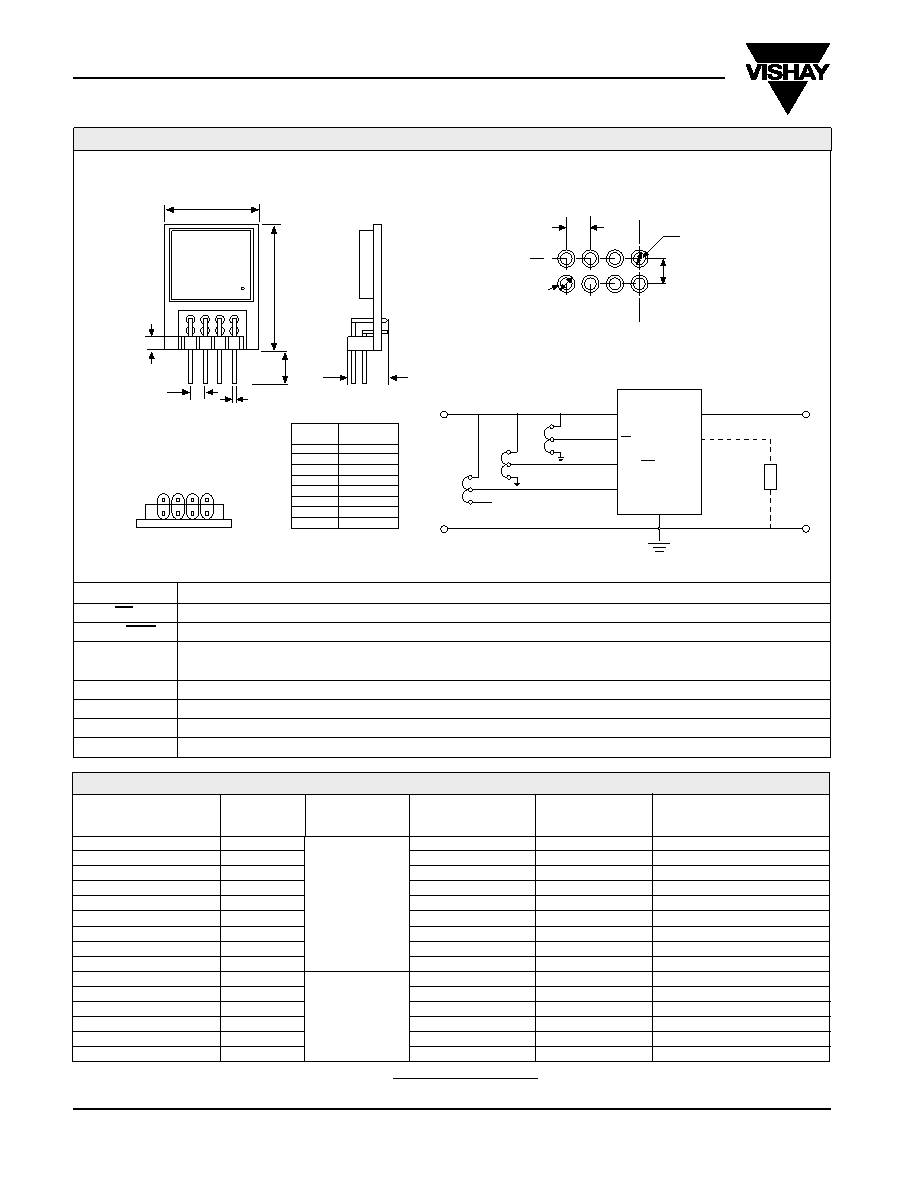
FX5545 GXXX XXX PI
Vishay
PIN
DESCRIPTION
SD
Logic low on SD pin shuts down the FunctionPAK completely and decreases current consumption to less than 1A.
PWM/PSM
Logic high =PWM mode, logic low =PSM mode. In PSM mode synchronous rectification is disabled.
SYNC
Externally controlled synchronization signal. Logic high to low transition forces the clock synchronization.
If not used the pin must be connected to Vin or logic high.
Vin
Input supply voltage
Vout
Output voltage
GND
Ground
Rext.
Included inside the package for all fixed output voltage converters. To be added externally for all self-selected output voltages.
SD
SYNC
Rext
Vin
DISABLE
ENABLE CONVERTER
Load
PWM
Vout
PSM
PWM/PSM
Vin
Rext
EXTERNAL
CLOCK
GND
PIN DESCRIPTION AND RECOMMENDED BOARD LAYOUT
MODEL
CIRCUIT
TYPE
DESCRIPTION
INPUT VOLTS
OUTPUT VOLTS
IDENTIFIER
@ AMPS
FX5545G001XVXPI
G001
1.5W, 0.6A
2.5 – 6.0
1.35 - 4.5* @ 0.6 max
FX5545G201XVXPI
G201
3W, 1.0A
2.5 – 6.0
1.35 - 4.5* @ 1.0 max
FX5545G018XVXPI
G018
3.6W, 3.0A
2.5 – 6.0
0.9 - 1.3 @ 3.0 max
FX5545G005XVXPI
G005
5W, 1.5A
2.5 – 6.0
1.35 - 4.5* @ 1.5 max
FX5545G105XVXPI
G105
6.5W, 2.0A
2.5 – 6.0
1.35 - 4.5* @ 2.0 max
FX5545G205XVXPI
G205
8W, 2.5A
2.5 – 6.0
1.35 - 4.5* @ 2.5 max
FX5545G008XVXPI**
G008
10W, 3.0A
2.5 – 6.0
0.9 - 4.5* @ 3.0 max
FX5545G305XVXPI
G305
10W, 3.0A
2.5 – 6.0
1.35 - 4.5* @ 3.0 max
FX5545G108XVXPI**
G108
15W, 4.0A
2.5 – 6.0
0.9 - 4.5* @ 4.0 max
FX5545G002XVXPI
G002
1.5W, 0.3A
2.5 – 6.0
3.3 - 6.0 @ 0.3 max
FX5545G202XVXPI
G202
3W, 0.6A
2.5 – 6.0
3.3 - 6.0 @ 0.6 max
FX5545G402XVXPI
G402
5W, 1.0A
2.5 – 6.0
3.3 - 6.0 @ 1.0 max
FX5545G006XVXPI
G006
9W, 1.5A
2.5 – 6.0
3.3 - 6.0 @ 1.5 max
FX5545G106XVXPI
G106
12W, 2.0A
2.5 – 6.0
3.3 - 6.0 @ 2.0 max
FX5545G206XVXPI
G206
15W, 2.5A
2.5 – 6.0
3.3 - 6.0 @ 2.5 max
DESIGN REFERENCE GUIDE - for details see www.vishay.com/integrated-modules/
*Note: For higher output voltage please consult factory at FunctionPAK@Vishay.com
**Note: FX5545G008ADJPI and FX5545G108ADJPI are available only at 1.35V - 4.5V output voltage
BUCK
BOOST
0.69 in
(17.5 mm)
0.98 in
0.23in
0.31 in
(25.0 mm)
(5.84 mm)
(7.9 mm)
0.1 in
(2.54 mm)
0.1 in
(2.54 mm)
PIn 1
PIN (0.64 mm)
View from bottom side
Use Standard Strip 0.1" (2.54 mm) Centers,
Double Row
All Positions Filled
Pad Recommended 0.060 in
0.1 in (2.54 mm)
Drill size
0.040 10 (1.02 mm)
0.1 in (2.54 mm)
8
1
5
4
RECOMMENDED BOARD LAYOUT
1
2
3
4
5
6
7
Vout
Vin
GND
Rext
SYNC
SD
PWM
GND
8
PIN No:
Description
相关PDF资料 |
PDF描述 |
|---|---|
| FX5545G2063V3PI | 1-OUTPUT 15 W DC-DC REG PWR SUPPLY MODULE |
| FX5545G0014V5PI | 1-OUTPUT 15 W DC-DC REG PWR SUPPLY MODULE |
| FX5545G1054V5PI | 1-OUTPUT 15 W DC-DC REG PWR SUPPLY MODULE |
| FX5545G0026V0PI | 1-OUTPUT 15 W DC-DC REG PWR SUPPLY MODULE |
| FX5545G0181V3PI | 1-OUTPUT 15 W DC-DC REG PWR SUPPLY MODULE |
相关代理商/技术参数 |
参数描述 |
|---|---|
| FX5545G0025V0PI | 功能描述:开关变换器、稳压器与控制器 BOOST 5V 1.5W PLUG-N RoHS:否 制造商:Texas Instruments 输出电压:1.2 V to 10 V 输出电流:300 mA 输出功率: 输入电压:3 V to 17 V 开关频率:1 MHz 工作温度范围: 安装风格:SMD/SMT 封装 / 箱体:WSON-8 封装:Reel |
| FX5545G0025V0T2 | 制造商:Vishay Intertechnologies 功能描述:Module DC-DC 1-OUT 5V 0.5A 1.5W 20-Pin BGA T/R |
| FX5545G0026V0 | 制造商:未知厂家 制造商全称:未知厂家 功能描述:Analog IC |
| FX5545G002ADJPI | 功能描述:开关变换器、稳压器与控制器 BOOST ADJV 1.5W PLUG RoHS:否 制造商:Texas Instruments 输出电压:1.2 V to 10 V 输出电流:300 mA 输出功率: 输入电压:3 V to 17 V 开关频率:1 MHz 工作温度范围: 安装风格:SMD/SMT 封装 / 箱体:WSON-8 封装:Reel |
| FX5545G005 | 制造商:VISHAY 制造商全称:Vishay Siliconix 功能描述:Industry Smallest and Low Profile 5W 1.5A DC/DC Buck Converter with High Output Power Density |
发布紧急采购,3分钟左右您将得到回复。