- 您现在的位置:买卖IC网 > PDF目录60214 > FX5545G005XVXSM (VISHAY INTERTECHNOLOGY INC) 1.5 A SWITCHING REGULATOR, QCC20 PDF资料下载
参数资料
| 型号: | FX5545G005XVXSM |
| 厂商: | VISHAY INTERTECHNOLOGY INC |
| 元件分类: | 稳压器 |
| 英文描述: | 1.5 A SWITCHING REGULATOR, QCC20 |
| 封装: | SMT-20 |
| 文件页数: | 1/3页 |
| 文件大小: | 172K |
| 代理商: | FX5545G005XVXSM |
Document Number: 10141
For technical questions, contact FunctionPAK@vishay.com
For marketing questions, contact FunctionPAK.marketing@vishay.com
www.vishay.com
Revision: 11-May-06
73
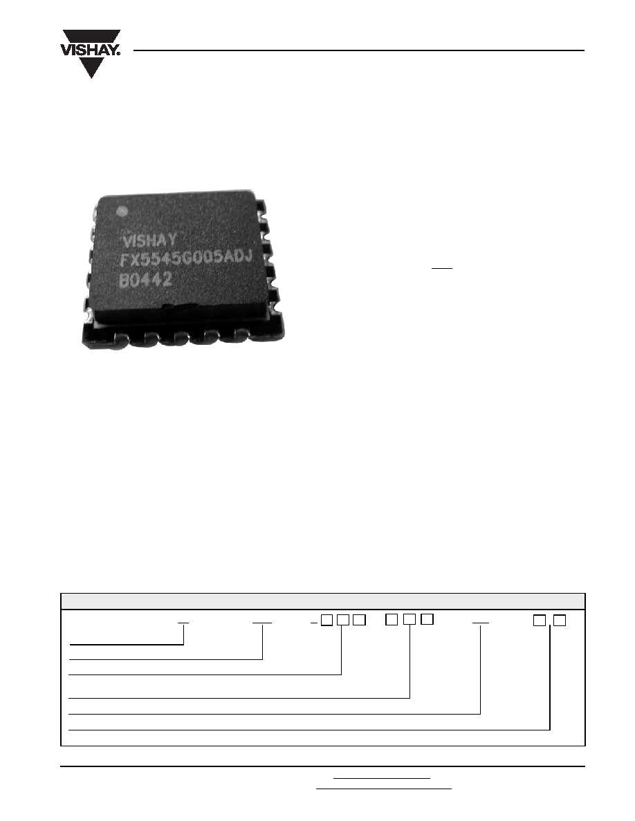
FX5545 GXXX XXX SM
Vishay
Fully Integrated DC/DC Converter 0.9V to 6V, 4A with
570W/in3 Power Density, Efficiency up to 95%.
Surface Mount Package for Prototyping
FEATURES
Fully integrated DC/DC converter
No external components required
Buck or Boost configurations
High efficiency over large load range
100% duty cycle
Power density - more than 570W/inch3
1A shutdown current
2.5V to 6V input range (1Li+ and 3-cell NiCd or NiMH cells)
0.9V to 6V output voltage
Programmable PWM/PSM controls
Low output ripple
Standard socket construction or plug-in for prototype
(use for BGA production)
Temperature range: - 40°C to + 85°C
Output power 15W
Maximum continuous current 4A
The
DC/DC
converter
is
a
programmable
topology
synchronized Buck or Boost converter for today’s continuous
changing electronic market. The DC/DC converter provides
flexibility of utilizing various battery configurations and
chemistries such as NiCd, NiMH, or Li+ with an input voltage
range of 2.5V to 6V. An additional flexibility is provided with
topology programmability to power multiple loads such as
power amplifiers, microcontrollers, or baseband logic IC’s.
For ultra-high efficiency, converters are designed to operate
in synchronous rectified PWM mode under full load while
transforming into externally controlled pulse-skipping mode
(PSM) under light load.
The DC/DC converter is available in 20-ports BGA package
for production. Convenient 8-pin plug-in modules are
available for prototyping. In order to satisfy the stringent
ambient temperature requirements, the DC/DC converter is
designed to handle the industrial temperature range of - 40°C
to + 85°C, with no cooling or derating.
APPLICATIONS (BGA)
Cordless phones, PDAs and others
Supply voltage source for low-voltage chip sets
Point of Load (POL) applications such as drivers for
FPGA’s, microprocessors, DSP’s, amplifiers, etc.
Portable computers
Battery back-up supplies
Cameras
* SM is the abbreviation for Surface Mount Package. The Surface Mount Package is designed for prototyping and not for volume usage.
ORDERING INFORMATION
FX
5545
G
SM*
FUNCTION
SIZE
CIRCUIT IDENTIFIER
OUTPUT VOLTAGE - Example: 2.7V should be written as 2V7 as the V indicates the
decimal point,or ADJ for adjustable version - self selectable output voltage.
SURFACE MOUNT VERSION
PACKAGING - B1 = 10pcs in bulk
For lead (Pb)-free solder please add E2 suffix
相关PDF资料 |
PDF描述 |
|---|---|
| FX5545G108XVXSM | 4 A SWITCHING REGULATOR, QCC20 |
| FX5545G106XVXSM | 2 A SWITCHING REGULATOR, QCC20 |
| FX5545G202XVXSM | 0.6 A SWITCHING REGULATOR, QCC20 |
| FX5545G006XVXSM | 1.5 A SWITCHING REGULATOR, QCC20 |
| FX5545G105XVXSM | 2 A SWITCHING REGULATOR, QCC20 |
相关代理商/技术参数 |
参数描述 |
|---|---|
| FX5545G006 | 制造商:VISHAY 制造商全称:Vishay Siliconix 功能描述:Industry Smallest and Low Profile 9W 1.5A DC/DC Boost Converter with High Output Power Density |
| FX5545G0062V7B1 | 制造商:VISHAY 制造商全称:Vishay Siliconix 功能描述:Industry Smallest and Low Profile 9W 1.5A DC/DC Boost Converter with High Output Power Density |
| FX5545G0062V7B1E2 | 制造商:VISHAY 制造商全称:Vishay Siliconix 功能描述:Industry Smallest and Low Profile 9W 1.5A DC/DC Boost Converter with High Output Power Density |
| FX5545G0062V7B5 | 制造商:VISHAY 制造商全称:Vishay Siliconix 功能描述:Industry Smallest and Low Profile 9W 1.5A DC/DC Boost Converter with High Output Power Density |
| FX5545G0062V7B5E2 | 制造商:VISHAY 制造商全称:Vishay Siliconix 功能描述:Industry Smallest and Low Profile 9W 1.5A DC/DC Boost Converter with High Output Power Density |
发布紧急采购,3分钟左右您将得到回复。