- 您现在的位置:买卖IC网 > PDF目录67594 > G1426F2U (Global Mixed-mode Technology Inc.) 2.2W Stereo Audio Amplifier PDF资料下载
参数资料
| 型号: | G1426F2U |
| 厂商: | Global Mixed-mode Technology Inc. |
| 元件分类: | 音频放大器 |
| 英文描述: | 2.2W Stereo Audio Amplifier |
| 中文描述: | 2.2W的立体声音频放大器 |
| 文件页数: | 6/13页 |
| 文件大小: | 282K |
| 代理商: | G1426F2U |
Ver: 1.0
Dec 04, 2003
TEL: 886-3-5788833
http://www.gmt.com.tw
2
G1426
Global Mixed-mode Technology Inc.
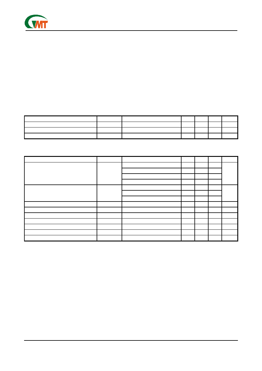
Absolute Maximum Ratings
Supply Voltage, VCC…………………..…...…….……...6V
Operating Ambient Temperature Range
TA…….…………………………….……….-40°C to +85°C
Maximum Junction Temperature, TJ…..……….….150°C
Storage Temperature Range, TSTG….….-65°C to+150°C
Soldering Temperature, 10seconds, TS……….……260°C
Power Dissipation
(1)
TA
≤ 25°C………………………………………….2.7W
TA
≤ 70°C………………………………………….1.7W
TA
≤ 85°C………………….………………………1.4W
Electrostatic Discharge, VESD
Human body mode..…………………….-3000 to 3000
(2)
Note:
(1) : Recommended PCB Layout
(2) : Human body model : C = 100pF, R = 1500, 3 positive pulses plus 3 negative pulses
Electrical Characteristics
DC Electrical Characteristics, VDD = 5.0V, TA=+25°C, unless otherwise noted
PARAMETER
SYMBOL
CONDITION
MIN
TYP
MAX
UNIT
Supply Current
IDD
VDD = 5V
-
8.5
15
mA
DC Differential Output Voltage
VO(DIFF)
VDD = 5V,Gain = 2
-
5
50
mV
IDD in Shutdown
ISD
VDD = 5V
-
0.1
2
A
(AC Operation Characteristics, VDD = 5.0V, TA=+25°C, RL = 4
, unless otherwise noted)
PARAMETER
SYMBOL
CONDITION
MIN
TYP
MAX
UNIT
THD = 1%, BTL, RL = 4
-
2
-
THD = 1%, BTL, RL = 8
-
1.25
-
THD = 10%, BTL, RL = 4
-
2.5
-
Output power (each channel) see Note
P(OUT)
THD = 10%, BTL, RL = 8
-
1.6
-
W
PO = 1.6W, BTL, RL = 4
-
300
-
PO = 1W, BTL, RL = 8
-
100
-
Total harmonic distortion plus noise
THD+N
VI = 1V, RL = 10K
, G = 1
-
10
-
m%
Maximum output power bandwidth
BOM
G = 10, THD = 1%
-
20
-
kHz
Phase margin
RL = 4
, Open Load
-
65
-
°
Power supply ripple rejection
PSRR
f = 120Hz
-
75
-
dB
Channel-to-channel output separation
f = 1kHz
-
80
-
dB
Input impedance
ZI
-
2
-
M
Signal-to-noise ratio
PO = 500mW, BTL
-
90
-
dB
Output noise voltage
Vn
Output noise voltage
-
55
-
V (rms)
Note :Output power is measured at the output terminals of the IC at 1kHz.
相关PDF资料 |
PDF描述 |
|---|---|
| G1426 | 2.2W Stereo Audio Amplifier |
| G1427F31UF | 2W Stereo Audio Amplifier |
| G1427F31U | 2W Stereo Audio Amplifier |
| G1427 | 2W Stereo Audio Amplifier |
| G1428 | 2W Stereo Audio Amplifier |
相关代理商/技术参数 |
参数描述 |
|---|---|
| G1427 | 功能描述:安装硬件 RG 2.5-72-12 3.000 DIA BLACK RoHS:否 制造商:Harwin 类型:SMT Cable Clip 材料:Phosphor Bronze 安装孔大小: 长度:5 mm 外径: 内径: 厚度: 电镀:Tin 螺纹大小: |
| G1427F31U | 制造商:GMT 制造商全称:Global Mixed-mode Technology Inc 功能描述:2W Stereo Audio Amplifier |
| G1427F31UF | 制造商:GMT 制造商全称:Global Mixed-mode Technology Inc 功能描述:2W Stereo Audio Amplifier |
| G1428 | 制造商:GMT 制造商全称:Global Mixed-mode Technology Inc 功能描述:2W Stereo Audio Amplifier |
| G1428F31U | 制造商:GMT 制造商全称:Global Mixed-mode Technology Inc 功能描述:2W Stereo Audio Amplifier |
发布紧急采购,3分钟左右您将得到回复。