- 您现在的位置:买卖IC网 > PDF目录64950 > G5910-50TBU (Global Mixed-mode Technology Inc.) High-Efficiency White LED Charge Pump PDF资料下载
参数资料
| 型号: | G5910-50TBU |
| 厂商: | Global Mixed-mode Technology Inc. |
| 英文描述: | High-Efficiency White LED Charge Pump |
| 中文描述: | 高效率白光LED电荷泵 |
| 文件页数: | 8/10页 |
| 文件大小: | 456K |
| 代理商: | G5910-50TBU |
Ver: 1.4
May 19, 2006
TEL: 886-3-5788833
http://www.gmt.com.tw
7
G5910
Global Mixed-mode Technology Inc.
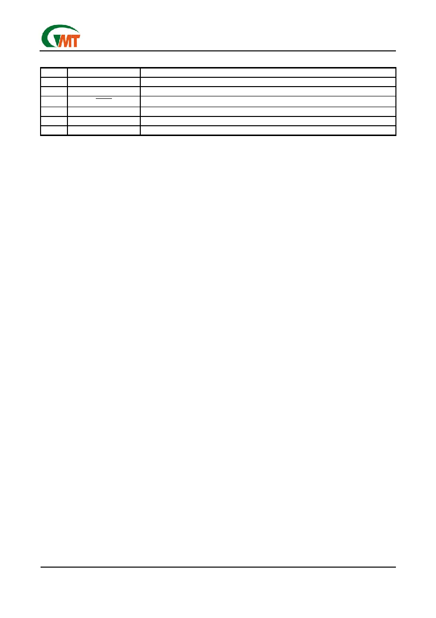
Pin Descriptions
PIN
NAME
FUNCTION
1
VOUT
Regulated output pin. Bypass this pin to ground with at least 6.8F low ESR capacitor
2
GND
Ground connection
3
SHDN
Shutdown input. Active low signal disables the converter.
4
C-
Flying capacitor negative terminal
5
VIN
Input supply pin. Bypass this pin to ground with at least 6.8F low ESR capacitor
6
C+
Flying capacitor positive terminal
Detailed Description
The G5910 uses a switched capacitor charge pump
to boost an input voltage to a regulated output volt-
age. Through an internal resistor divider network
the output regulation is achieved by sensing the
charge pump output voltage. When the divided
output drops below a preset trip point that con-
trolled by an internal comparator a switched dou-
bling circuit is enabled. The charge pump switch
cycling enables four internal switches at two
non-overlapping phases. During the first phase,
switches S1 and S4 are switched on (short) and
switch S2 and S3 are off (open). The flying capaci-
tor CFLY is charged to a level approximately equal to
input voltage VIN. On the second phase, switches
S1 and S4 are turned off (open), S2 and S3 are
turned on (short). During the first phase the low
side of the flying capacitor CFLY is connected to
GND. During the second phase, the flying capacitor
CFLY is switched so that the low side is connected to
VIN. The voltage at the high side of the flying ca-
pacitor CFLY is bootstrapped to 2 × VIN and is con-
nected to output through a switch. For each cycle
phase, charge from input node VIN is transported
from a lower voltage to a higher voltage. This cycle
repeats itself until the output node voltage is high
enough to exceed the preset input threshold of the
control comparator. When the output voltage ex-
ceeds the internal trip point voltage level, the
switching cycle stops and the charge pump circuit is
placed in an idle state. The closed loop feed back
system containing the voltage sense circuit and
control comparator allows the G5910 to provide a
regulated output voltage and output load current.
An integrated oscillator within the control circuit
block creates the switching signal that drives the
charge pump. The free running charge pump
switching frequency is approximately 1MHz. The
G5910 has complete output short circuit and ther-
mal protection to safeguard the device under ex-
treme operating conditions. When output voltage is
short to ground, the switches S1, S4, and S3 are
turned on with limited current of 220mA. After the
short circuit condition has been released and output
voltage rises above a threshold voltage, the G5910
will go into normal operation mode. An internal
thermal protection circuit senses die temperature
and will shut down the device if the internal junction
temperature exceeds approximately 150°C. The
charge pump will remain disabling until the fault
condition is relieved.
相关PDF资料 |
PDF描述 |
|---|---|
| G5910 | High-Efficiency White LED Charge Pump |
| G684 | Microprocessor Reset IC |
| G6854-01 | InGaAs PIN photodiode |
| G696L263T | Microprocessor Reset IC |
| G696L293T | Microprocessor Reset IC |
相关代理商/技术参数 |
参数描述 |
|---|---|
| G5910-50TPU | 制造商:GMT 制造商全称:Global Mixed-mode Technology Inc 功能描述:High-Efficiency White LED Charge Pump |
| G592 | 制造商:SLI EBT 功能描述:LAMP G3.1/2 MES 24V 1.2W |
| G5920 | 制造商:GMT 制造商全称:Global Mixed-mode Technology Inc 功能描述:Ultra Low-Dropout, Constant-Current White LED Bias |
| G5920TB1U | 制造商:GMT 制造商全称:Global Mixed-mode Technology Inc 功能描述:Ultra Low-Dropout, Constant-Current White LED Bias |
| G5921 | 制造商:GMT 制造商全称:Global Mixed-mode Technology Inc 功能描述:Ultra Low-Dropout, Constant-Current White LED Bias |
发布紧急采购,3分钟左右您将得到回复。