- 您现在的位置:买卖IC网 > PDF目录60277 > G910T21UF (Global Mixed-mode Technology Inc.) Cap-Free, NMOS, 150mA Low Dropout Regulator with Reverse Current Protection PDF资料下载
参数资料
| 型号: | G910T21UF |
| 厂商: | Global Mixed-mode Technology Inc. |
| 元件分类: | 线性稳压 |
| 英文描述: | Cap-Free, NMOS, 150mA Low Dropout Regulator with Reverse Current Protection |
| 中文描述: | 无电容,NMOS管,150mA的低压差稳压器的反向电流保护 |
| 文件页数: | 3/10页 |
| 文件大小: | 416K |
| 代理商: | G910T21UF |
Ver: 7.2
Jan 20, 2006
TEL: 886-3-5788833
http://www.gmt.com.tw
2
G910/G911
Global Mixed-mode Technology Inc.
Absolute Maximum Ratings
(Note 1)
Input Voltage. . . . . . . . . . . . . . . . . . . . . . . . . . . . . . . 7V
Power Dissipation Internally Limited
(Note2)
Maximum Junction Temperature . . . . . . . . . . . . .150°C
Storage Temperature Range. . . . . -65°C
≤ TJ ≤+150°C
Reflow Temperature (soldering, 10sec) . . . . . . .260°C
Thermal Resistance Junction to Ambient, (θJA)
SOT-89. . . . . . . . . . . . . . . . . . . . . . . . . . . . . 173°C/W(1)
SOT-223. . . . . . . . . . . . . . . . . . . . . . . . . . . . 148°C/W(1)
TO-92, TO-92 . . . . . . . . . . . . . . . . . . . . . . .159°C/W(1)
Thermal Resistance Junction to Case, (θJc)
SOT-89. . . . . . . . . . . . . . . . . . . . . . . . . . . . . . ..25°C/W
SOT-223 . . . . . . . . . . . . . . . . . . . . . .. . . . . . . . 22°C/W
Note (1): See Recommended Minimum Footprint.
Operating Conditions
(Note 1)
Input Voltage. . . . . . . . . . . . . . . . . . . . . . . . . 4V ~ 6.5V
Temperature Range . . . . . . . . . . . . .-40°C
≤ TA ≤85°C
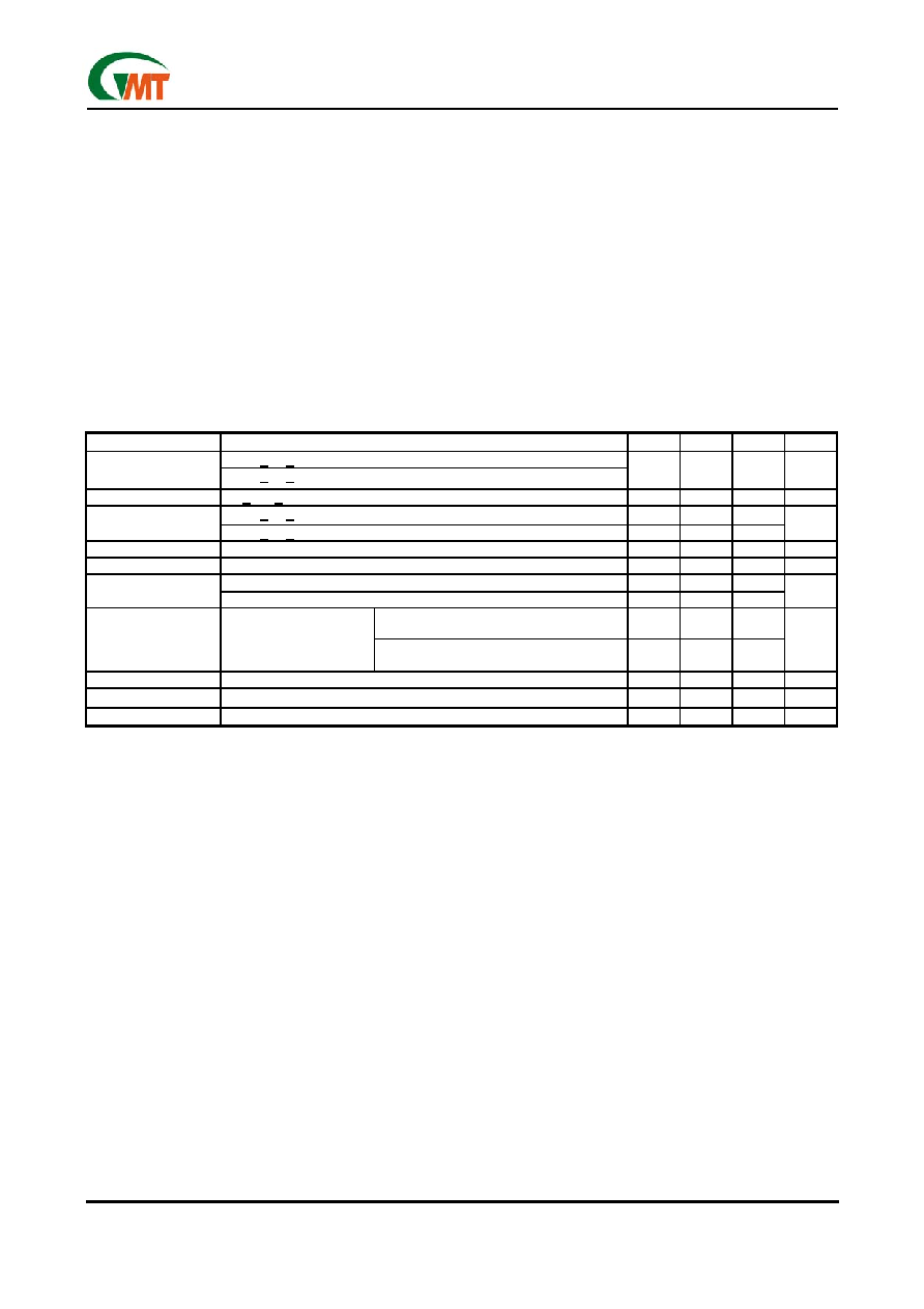
Electrical Characteristics
VIN =5V, IO = 600mA/250mA+, CIN=10F, COUT =10F. All specifications apply for TA = TJ = 25°C.[Note 3]
PARAMETER
CONDITION
MIN
TYP
MAX
UNIT
10mA < IO <600mA
Output Voltage
10mA < IO <250mA
+
3.234
3.3
3.366
V
Line Regulation
4V < VIN < 6V, IO = 10mA
---
15
---
mV
10mA < IO < 600mA
---
20
---
Load Regulation
10mA < IO < 250mA
+
---
10
---
mV
Quiescent Current
VIN = 5V
---
0.3
---
mA
Ripple Rejection
fi = 120 Hz, 1VP-P, Io = 100mA
---
47
---
dB
IO = 600mA
---
0.65
---
Dropout Voltage
IO = 250mA
+
---
0.25
---
V
VIN = 4.5V, mounted on SOT-89 recom-
mended minimum footprint
---
600
---
Output Current
Continuous Test
TA = 25°C, TJ < 125°C,
VOUT within ±2% (Note 2) VIN = 5.2V, TO-92 & TO-92 package
0.53 inch leads soldered to PC Board
---
250+
---
mA
Short Circuit Current
---
0.65
---
A
Current Limit
0.8
A
Over Temperature
---
145
---
°C
[
+
for
TO-92 & TO-92 Package]
Note 1:
Absolute Maximum Ratings are limits beyond which damage to the device may occur. Operating Conditions are condi-
tions under which the device functions but the specifications might not be guaranteed. For guaranteed specifications and
test conditions see the Electrical Characteristics.
Note2:
The maximum power dissipation is a function of the maximum junction temperature, TJmax ; total thermal resistance, θJA,
and ambient temperature TA. The maximum allowable power dissipation at any ambient temperature is Tjmax-TA / θJA. If this
dissipation is exceeded, the die temperature will rise above 150°C and IC will go into thermal shutdown. For the G910 in
TO-92, TO-92,
θJA is 159°C/W ;in the SOT-223 package is 148°C/W and SOT-89 package is 173°C/W (See Recom-
mended Minimum Footprint). The safe operation in TO-92 & TO-92 package, it can see “Typical Performance Charac-
teristics” (Safe Operating Area).
Note3:
Low duty pulse techniques are used during test to maintain junction temperature as close to ambient as possible.
Note4:
The type of output capacitor should be tantalum or aluminum.
Definitions
Dropout Voltage
The input/output Voltage differential at which the regu-
lator output no longer maintains regulation against
further reductions in input voltage. Measured when the
output drops 100mV below its nominal value, dropout
voltage is affected by junction temperature, load cur-
rent and minimum input supply requirements.
Line Regulation
The change in output voltage for a change in input volt-
age. The measurement is made under conditions of low
dissipation or by using pulse techniques such that av-
erage chip temperature is not significantly affected.
Load Regulation
The change in output voltage for a change in load
current at constant chip temperature. The measure-
ment is made under conditions of low dissipation or by
using pulse techniques such that average chip tem-
perature is not significantly affected.
Maximum Power Dissipation
The maximum total device dissipation for which the
regulator will operate within specifications.
Quiescent Bias Current
Current which is used to operate the regulator chip
and is not delivered to the load.
相关PDF资料 |
PDF描述 |
|---|---|
| G910T21U | Cap-Free, NMOS, 150mA Low Dropout Regulator with Reverse Current Protection |
| G910T22B | Cap-Free, NMOS, 150mA Low Dropout Regulator with Reverse Current Protection |
| G910T22D | Cap-Free, NMOS, 150mA Low Dropout Regulator with Reverse Current Protection |
| G910T22T | Cap-Free, NMOS, 150mA Low Dropout Regulator with Reverse Current Protection |
| G910T22U | Cap-Free, NMOS, 150mA Low Dropout Regulator with Reverse Current Protection |
相关代理商/技术参数 |
参数描述 |
|---|---|
| G910T22B | 制造商:GMT 制造商全称:Global Mixed-mode Technology Inc 功能描述:3.3V 400mA/250mA Low Dropout Regulator |
| G910T22D | 制造商:GMT 制造商全称:Global Mixed-mode Technology Inc 功能描述:3.3V 400mA/250mA Low Dropout Regulator |
| G910T22T | 制造商:GMT 制造商全称:Global Mixed-mode Technology Inc 功能描述:3.3V 400mA/250mA Low Dropout Regulator |
| G910T22U | 制造商:GMT 制造商全称:Global Mixed-mode Technology Inc 功能描述:3.3V 400mA/250mA Low Dropout Regulator |
| G910T23B | 制造商:GMT 制造商全称:Global Mixed-mode Technology Inc 功能描述:3.3V 400mA/250mA Low Dropout Regulator |
发布紧急采购,3分钟左右您将得到回复。