- 您现在的位置:买卖IC网 > PDF目录4115 > GAL22V10D-25QJN (Lattice Semiconductor Corporation)SPLD GAL 10 MACRO CELLS 38.5MHZ PDF资料下载
参数资料
| 型号: | GAL22V10D-25QJN |
| 厂商: | Lattice Semiconductor Corporation |
| 文件页数: | 7/23页 |
| 文件大小: | 0K |
| 描述: | SPLD GAL 10 MACRO CELLS 38.5MHZ |
| 产品变化通告: | Product Discontinuation 07/Sept/2010 |
| 标准包装: | 370 |
| 可编程类型: | EE PLD |
| 宏单元数: | 10 |
| 输入电压: | 4.75 V ~ 5.25 V |
| 速度: | 25ns |
| 安装类型: | 表面贴装 |
| 封装/外壳: | 28-LCC(J 形引线) |
| 供应商设备封装: | 28-PLCC(11.51x11.51) |
| 包装: | 托盘 |
| 其它名称: | Q6613932 |
Specifications GAL22V10
13
Electronic Signature
An electronic signature (ES) is provided in every GAL22V10
device. It contains 64 bits of reprogrammable memory that can
contain user-defined data. Some uses include user ID codes,
revision numbers, or inventory control. The signature data is
always available to the user independent of the state of the se-
curity cell.
The electronic signature is an additional feature not present in
other manufacturers' 22V10 devices. To use the extra feature of
the user-programmable electronic signature it is necessary to
choose a Lattice Semiconductor 22V10 device type when com-
piling a set of logic equations. In addition, many device program-
mers have two separate selections for the device, typically a
GAL22V10 and a GAL22V10-UES (UES = User Electronic Sig-
nature) or GAL22V10-ES. This allows users to maintain compat-
ibility with existing 22V10 designs, while still having the option to
use the GAL device's extra feature.
The JEDEC map for the GAL22V10 contains the 64 extra fuses
for the electronic signature, for a total of 5892 fuses. However,
the GAL22V10 device can still be programmed with a standard
22V10 JEDEC map (5828 fuses) with any qualified device pro-
grammer.
Security Cell
A security cell is provided in every GAL22V10 device to prevent
unauthorized copying of the array patterns. Once programmed,
this cell prevents further read access to the functional bits in the
device. This cell can only be erased by re-programming the
device, so the original configuration can never be examined once
this cell is programmed. The Electronic Signature is always avail-
able to the user, regardless of the state of this control cell.
Latch-Up Protection
GAL22V10 devices are designed with an on-board charge pump
to negatively bias the substrate. The negative bias is of sufficient
magnitude to prevent input undershoots from causing the circuitry
to latch. Additionally, outputs are designed with n-channel pullups
instead of the traditional p-channel pullups to eliminate any pos-
sibility of SCR induced latching.
Device Programming
GAL devices are programmed using a Lattice Semiconductor-
approved Logic Programmer, available from a number of manu-
facturers (see the the GAL Development Tools section). Com-
plete programming of the device takes only a few seconds. Eras-
ing of the device is transparent to the user, and is done automati-
cally as part of the programming cycle.
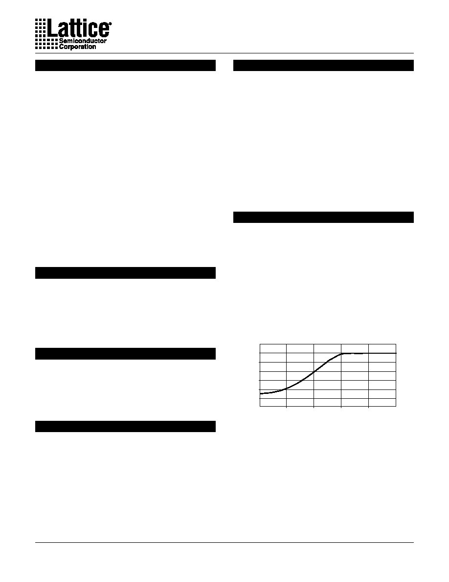
Typical Input Current
1 .0
2 .0
3 .0
4 .0
5 .0
-6 0
0
-2 0
-4 0
0
Input V olt age ( V olt s)
Input
C
ur
re
nt
(
uA
)
Output Register Preload
When testing state machine designs, all possible states and state
transitions must be verified in the design, not just those required
in the normal machine operations. This is because certain events
may occur during system operation that throw the logic into an
illegal state (power-up, line voltage glitches, brown-outs, etc.). To
test a design for proper treatment of these conditions, a way must
be provided to break the feedback paths, and force any desired
(i.e., illegal) state into the registers. Then the machine can be
sequenced and the outputs tested for correct next state condi-
tions.
The GAL22V10 device includes circuitry that allows each regis-
tered output to be synchronously set either high or low. Thus, any
present state condition can be forced for test sequencing. If
necessary, approved GAL programmers capable of executing test
vectors perform output register preload automatically.
Input Buffers
GAL22V10 devices are designed with TTL level compatible in-
put buffers. These buffers have a characteristically high imped-
ance, and present a much lighter load to the driving logic than bi-
polar TTL devices.
The input and I/O pins also have built-in active pull-ups. As a re-
sult, floating inputs will float to a TTL high (logic 1). However,
Lattice Semiconductor recommends that all unused inputs and
tri-stated I/O pins be connected to an adjacent active input, Vcc,
or ground. Doing so will tend to improve noise immunity and
reduce Icc for the device. (See equivalent input and I/O schemat-
ics on the following page.)
ALL
DEVICES
DISCONTINUED
相关PDF资料 |
PDF描述 |
|---|---|
| AMC36DRAI-S734 | CONN EDGECARD 72POS .100 R/A PCB |
| ESC50DTEF | CONN EDGECARD 100POS .100 EYELET |
| GAL16V8D-25LP | IC GAL 8OUT MACROCELL 3.5NS 20DI |
| IDT7143LA90J8 | IC SRAM 32KBIT 90NS 68PLCC |
| ATF20V8BQL-15JU | IC PLD 15NS 28PLCC |
相关代理商/技术参数 |
参数描述 |
|---|---|
| GAL22V10D-25QP | 功能描述:SPLD - 简单可编程逻辑器件 5V 22 I/O RoHS:否 制造商:Texas Instruments 逻辑系列:TICPAL22V10Z 大电池数量:10 最大工作频率:66 MHz 延迟时间:25 ns 工作电源电压:4.75 V to 5.25 V 电源电流:100 uA 最大工作温度:+ 75 C 最小工作温度:0 C 安装风格:Through Hole 封装 / 箱体:DIP-24 |
| GAL22V10D25QPN | 制造商:Lattice Semiconductor Corporation 功能描述: |
| GAL22V10D-25QPN | 功能描述:SPLD - 简单可编程逻辑器件 HI PERF E2CMOS PLD RoHS:否 制造商:Texas Instruments 逻辑系列:TICPAL22V10Z 大电池数量:10 最大工作频率:66 MHz 延迟时间:25 ns 工作电源电压:4.75 V to 5.25 V 电源电流:100 uA 最大工作温度:+ 75 C 最小工作温度:0 C 安装风格:Through Hole 封装 / 箱体:DIP-24 |
| GAL22V10D-30LD/883 | 制造商:未知厂家 制造商全称:未知厂家 功能描述:Electrically-Erasable PLD |
| GAL22V10D-4LJ | 功能描述:SPLD - 简单可编程逻辑器件 HI PERF E2CMOS PLD RoHS:否 制造商:Texas Instruments 逻辑系列:TICPAL22V10Z 大电池数量:10 最大工作频率:66 MHz 延迟时间:25 ns 工作电源电压:4.75 V to 5.25 V 电源电流:100 uA 最大工作温度:+ 75 C 最小工作温度:0 C 安装风格:Through Hole 封装 / 箱体:DIP-24 |
发布紧急采购,3分钟左右您将得到回复。