参数资料
| 型号: | GDBD4410 |
| 厂商: | IXYS |
| 文件页数: | 4/6页 |
| 文件大小: | 0K |
| 描述: | BOARD EVALUATION IXBD4410/11 |
| 标准包装: | 2 |
| 类型: | 电源管理:MOSFET 驱动器 |
| 适用于相关产品: | IXBD4410,IXBD4411 |
| 所含物品: | 评估板 |
�� �
�
�GDBD� 4410�
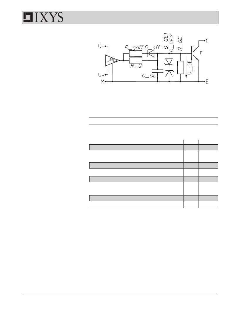
�On� board� gate� resistors� of� R� Gint� =� 4,7� ?� are�
�provided� between� the� outputs� of� the� IXBD4410/�
�4411� ICs� and� the� respective� terminals� g1...g7.�
�Total� gate� resistance� R� G� for� operation� of� the�
�IGBTs� should� be� adjusted� by� addition� of� an�
�external� gate� resistor� R� Gext� in� each� gate� wire� on�
�the� printed� circuit� board,� connecting� the� driver�
�unit� and� the� CBI� module,� according� to:�
�R� G� =� R� Gint� +� R� Gext�
�It� is� recommended� to� use� total� gate� resistors�
�R� G� for� inverter� and� brake� chopper� as� specified�
�in� the� respective� module� data� sheets.� Circuitry�
�according� to� figure� 1� may� be� added� to� adjust�
�current� and� voltage� change� rates� during�
�commutations� and� for� protection� purposes.�
�Figure� 1:� optional� gate� circuitry� between� driver� unit� and� CBI� module�
�Protection� Schemes�
�Symbol�
�Definitions�
�Max.� Ratings�
�To� assure� maximum� protection� for� the� power�
�devices,� the� driver� unit� incorporates� the� following�
�V� DD� /V� EE�
�Supply� Voltage�
�-0.5� ...� 24�
�V�
�IGBT� protection� schemes:�
�?� protection� from� cross� conduction� of� the� half�
�bridge,� see� section� Logic� Interfaces�
�?� power� device� overcurrent� or� desaturation�
�Symbol�
�Definitions/Conditions�
�Characteristic� Values�
�(T� VJ� =� 25°C,� V� DD� =� 15� V� unless� otherwise� specified)�
�min.� typ.�
�max.�
�protection:� The� IXBD4410/4411� IC� will� turn�
�off� the� driven� device,� supposed� to� be� turned�
�V� DD� Undervoltage� Lockout�
�on� since� at� least� 3� μs� typ.,� within� 150� ns� of�
�sensing� an� output� overcurrent� or� desaturation�
�condition,� i.� e.� U� CE� >10� V� typ.� Measurement�
�V� uv�
�V� uh�
�Drop� out�
�Hysteresis�
�9.5�
�0.1�
�10.5�
�0.15�
�11.5�
�0.3�
�V�
�V�
�is� taken� with� a� resistive� voltage� divider,�
�limiting� device� blocking� and� thus� DC� link�
�VEE� Supply� (referred� to� M2467/M1/M3/M5)�
�voltage� to� U� Z� =� 800V.�
�V� EEF�
�Over-voltage� fault� indication�
�-4.8�
�-3�
�V�
�?� under-voltage� gate-drive� lockout� on� the� low-�
�and/or� high-� side� drivers� whenever� the�
�Open� Drain� Fault� Output� (referred� to� M2467)�
�respective� positive� power� supply� V� DD� falls�
�below� 9.5� V� typically�
�?� over-voltage� gate-drive� lockout� on� the� low-�
�V� oh�
�V� ol�
�HI� output� /� R� pu� =� 10� k� ?� to� V� DD�
�LO� output� /� I� o� =� 4� mA�
�V� DD� -0.05�
�0.3�
�0.5�
�V�
�V�
�and� high-� side� drivers� whenever� the� respective�
�negative� power� supply� V� EE� rises� above� -3� V�
�Quiescent� Power� Supply� Current� per� Driver� IC�
�typically,� cf.� section� Transistor� Drive�
�?� During� power-up,� the� chipset’s� gate-drive�
�I� DD�
�V� DD� current� /� V� in� =� V� DD� or� LG,� I� o� =� 0�
�20�
�mA�
�outputs� will� be� low� (off),� until� the� voltage�
�reaches� the� supply� voltage� trip� points.�
�During� a� status� fault,� high� side� or� low� side� driver�
�IC� of� the� concerned� phaselegs� keep� their�
�respective� outputs� off� at� V� EE� as� long� as� supplied.�
�The� overcurrent� fault� condition� is� latched,�
�which� is� reset� on� the� next� positive� transition� of�
�the� respective� input� PBM1...PBM7,� provided�
�that� the� fault� condition� is� not� applicable� any�
�more.�
�Further� the� driver� unit� provides� a� logic�
�compatible� fault� indication:� Activation� of� open�
�drain� output� F indicates� a� fault� in� any� of� the� low�
�or� high� side� drivers.� This� signal� can� be� utilised�
�by� a� superceeding� control� unit� on� ground� –� i.e.�
�DC� link� minus� –� potential,� e.g.� a� microprocessor.�
�The� high� level� when� F is� not� activated� should�
�be� supplied� by� an� external� pull� up� resistor�
�connected� to� the� appropriate� supply� voltage.�
�?� 2004� IXYS� All� rights� reserved�
�4-6�
�相关PDF资料 |
PDF描述 |
|---|---|
| GH1250 | FUSE INDUST 1250A 550V 84X198MM |
| GMF.3K.085.EANZ | RUBBER BOOT |
| GPIODM-KPLCD | BOARD DEMO LCD GPIO EXP KEYPAD |
| GSAP 15-R | FUSE 15A 250VAC AXIAL SLOW |
| GSB3211311WEU | USB 3.0 DIP B RECP THRU HOLE |
相关代理商/技术参数 |
参数描述 |
|---|---|
| GDBE111630-19 | 制造商:ITT Interconnect Solutions 功能描述:GDBE111630-19 - Bulk |
| GDBE-25S-A156 | 制造商:ITT Interconnect Solutions 功能描述:GDBE-25S-A156 - Bulk |
| GDB-V-1.25A | 制造商:Cooper Bussmann 功能描述:Fuse Miniature 1.25A 250V Fast 2-Pin Axial Through Hole Cardboard Carton |
| GDB-V-1.6A | 制造商:Cooper Bussmann 功能描述: |
| GDB-V-100MA | 制造商:Cooper Bussmann 功能描述: |
发布紧急采购,3分钟左右您将得到回复。