- 您现在的位置:买卖IC网 > PDF目录223854 > GL602USB (Electronic Theatre Controls, Inc.) USB KEYBOARD MICROCONTROLLER PDF资料下载
参数资料
| 型号: | GL602USB |
| 厂商: | Electronic Theatre Controls, Inc. |
| 英文描述: | USB KEYBOARD MICROCONTROLLER |
| 中文描述: | USB键盘单片机 |
| 文件页数: | 13/35页 |
| 文件大小: | 201K |
| 代理商: | GL602USB |
第1页第2页第3页第4页第5页第6页第7页第8页第9页第10页第11页第12页当前第13页第14页第15页第16页第17页第18页第19页第20页第21页第22页第23页第24页第25页第26页第27页第28页第29页第30页第31页第32页第33页第34页第35页
Revision 1.6
-20-
02/28/2000
0.0
0.2
0.4
0.6
0.8
1.0
0.0
0.2
0.4
0.6
0.8
1.0
1.2
1.4
1.6
1.8
2.0
2.2
2.4
2.6
2.8
3.0
3.2
Common Mode Input Voltage (volts)
Mi
nim
u
m
D
if
fe
re
n
ti
a
lS
e
ns
it
iv
it
y
(
v
ol
ts
)
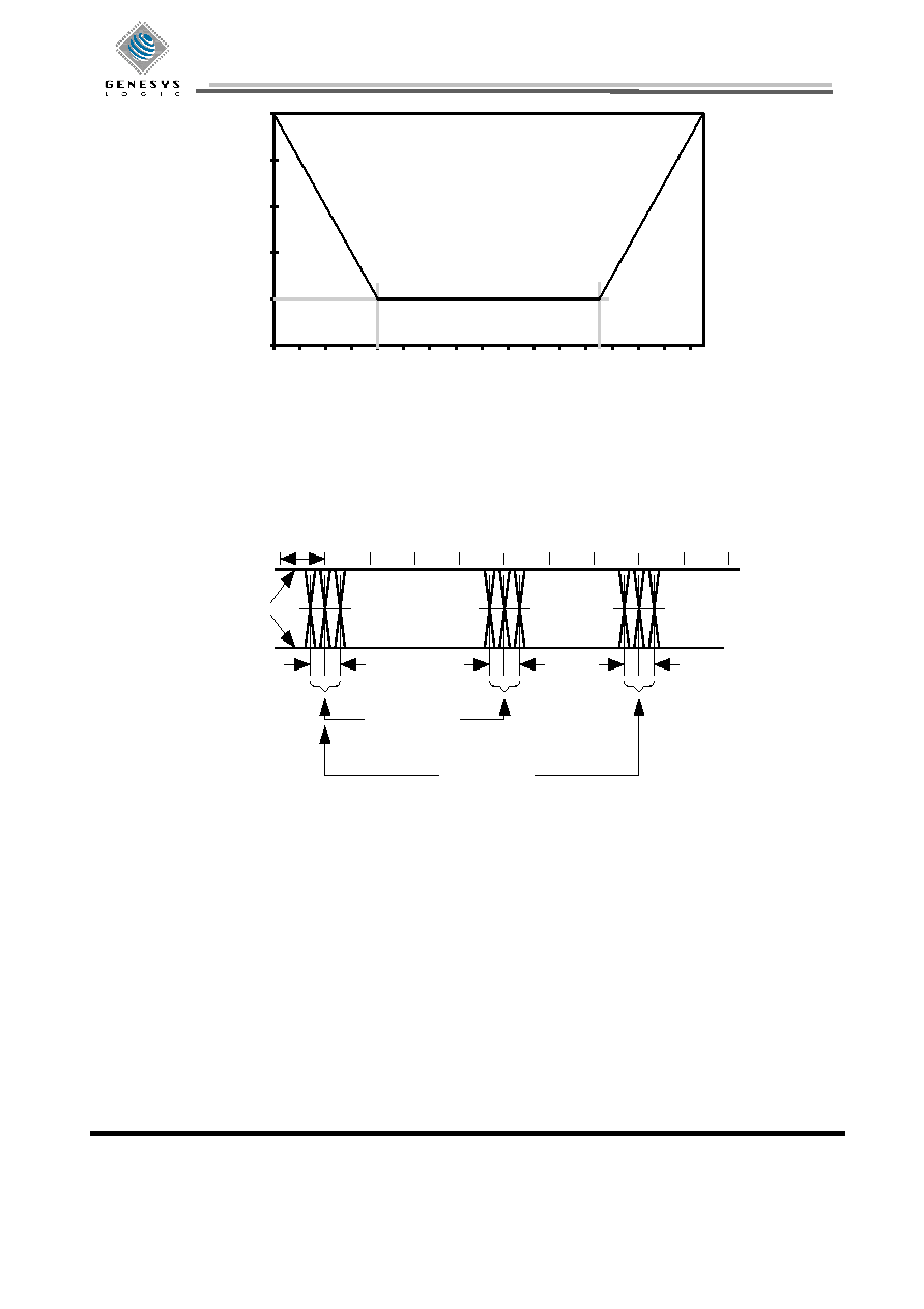
Figure 4-3 Differential Input Sensitivity over Entire Common Mode Range
The data receivers for all types of devices must be able to properly decode the differential data in the presence of
jitter. The more of the bit time that any data edge can occupy and still be decoded, the more reliable the data
transfer will be. Data receivers are required to decode differential data transitions that occur in a window plus and
minus a nominal quarter bit time from the nominal (centered) data edge position. Jitter will be caused by the delay
mismatches and by mismatches in the source and destination data rates (frequencies).
D
Diiffffe
erre
en
nttiia
all
D
Da
atta
a L
Liin
ne
es
s
P
Pa
aiirre
ed
d
T
Trra
an
ns
siittiio
on
ns
s
N
N ** T
TPPEER
RIIO
OD
D
+
+ T
TJJR
R2
2
T
TPPEERRIIO
OD
D
C
Co
on
ns
se
ec
cu
uttiiv
ve
e
T
Trra
an
ns
siittiio
on
ns
s
N
N ** T
TPPEER
RIIO
OD
D +
+ T
TJJR
R1
1
T
TJJR
R
T
TJJR
R1
1
T
TJJR
R2
2
Figure 4-4 Receiver Jitter Tolerance
The source of data can have some variation (jitter) in the timing of edges of the data transmitted. The time between
any set of data transitions is N*TPeriod ± jitter time, where N is the number of bits between the transitions and TPeriod
is defined as the actual period of the data rate. The data jitter is measured with the same capacitive load used for
maximum rise and fall times and is measured at the crossover points of the data lines.
For low-speed transmissions, the jitter time for any consecutive differential data transitions must be within
±25ns
and within
±10ns for any set of paired differential data transitions. These jitter numbers include timing variations
due to differential buffer delay, rise/fall time mismatches, internal clock source jitter, noise and other random
effects.
The output rise time and fall time are measured between 10% and 90% of the signal. Edge transition time for the
rising and falling edges of low-speed signals is 75ns (minimum) into a capacitive load (CL) of 50pF and 300ns
(maximum) into a capacitive load of 350pF. The rising and falling edges should be transitioning (monotonic)
smoothly when driving the cable to avoid excessive EMI.
相关PDF资料 |
PDF描述 |
|---|---|
| GL602USB-A | USB KEYBOARD MICROCONTROLLER |
| GL9575 | P-CHANNEL ENHANCEMENT MODE POWER MOSFET |
| GLCB03A9A5C029 | SNAP ACTING/LIMIT SWITCH, SPDT, MOMENTARY, 0.55A, 125VDC, PANEL MOUNT |
| GLCB04A9A1C026 | SNAP ACTING/LIMIT SWITCH, SPDT, MOMENTARY, 0.55A, 125VDC, PANEL MOUNT |
| GLCB04A9A1Q02 | SNAP ACTING/LIMIT SWITCH, SPDT, MOMENTARY, 0.55A, 125VDC, PANEL MOUNT |
相关代理商/技术参数 |
参数描述 |
|---|---|
| GL602USB-A | 制造商:未知厂家 制造商全称:未知厂家 功能描述:USB KEYBOARD MICROCONTROLLER |
| GL603USB | 制造商:未知厂家 制造商全称:未知厂家 功能描述:USB + PS/2 MOUSE MICROCONTROLLER |
| GL603USB-A | 制造商:未知厂家 制造商全称:未知厂家 功能描述:USB + PS/2 MOUSE MICROCONTROLLER |
| GL603USB-B | 制造商:未知厂家 制造商全称:未知厂家 功能描述:USB + PS/2 MOUSE MICROCONTROLLER |
| GL6100 | 制造商:SIERRA WIRELESS 功能描述:MODEM KIT GPRS RS232 ANTENNA 制造商:SIERRA WIRELESS 功能描述:MODEM, GSM / GPRS, QUAD BAND, RS232 制造商:SIERRA WIRELESS 功能描述:MODEM, GSM / GPRS, QUAD BAND, RS232; Protocol:TCP / IP; Supply Voltage Min:4.75V; Supply Voltage Max:32V; Module Interface:Serial; Kit Features:Quad Band 850/900/1800/1900 MHz GSM-GPRS Class 10 Modem, CSD, Fax and SMS; Supply Voltage;RoHS Compliant: Yes |
发布紧急采购,3分钟左右您将得到回复。