- 您现在的位置:买卖IC网 > PDF目录383012 > GM72V66841ET-7K (HYNIX SEMICONDUCTOR INC) 2,097,152 WORD x 8 BIT x 4 BANK SYNCHRONOUS DYNAMIC RAM PDF资料下载
参数资料
| 型号: | GM72V66841ET-7K |
| 厂商: | HYNIX SEMICONDUCTOR INC |
| 元件分类: | DRAM |
| 英文描述: | 2,097,152 WORD x 8 BIT x 4 BANK SYNCHRONOUS DYNAMIC RAM |
| 中文描述: | 8M X 8 SYNCHRONOUS DRAM, 6 ns, PDSO54 |
| 封装: | 0.400 INCH, TSOP2-54 |
| 文件页数: | 4/57页 |
| 文件大小: | 592K |
| 代理商: | GM72V66841ET-7K |
第1页第2页第3页当前第4页第5页第6页第7页第8页第9页第10页第11页第12页第13页第14页第15页第16页第17页第18页第19页第20页第21页第22页第23页第24页第25页第26页第27页第28页第29页第30页第31页第32页第33页第34页第35页第36页第37页第38页第39页第40页第41页第42页第43页第44页第45页第46页第47页第48页第49页第50页第51页第52页第53页第54页第55页第56页第57页
LG Semicon
GM72V66841CT/CLT
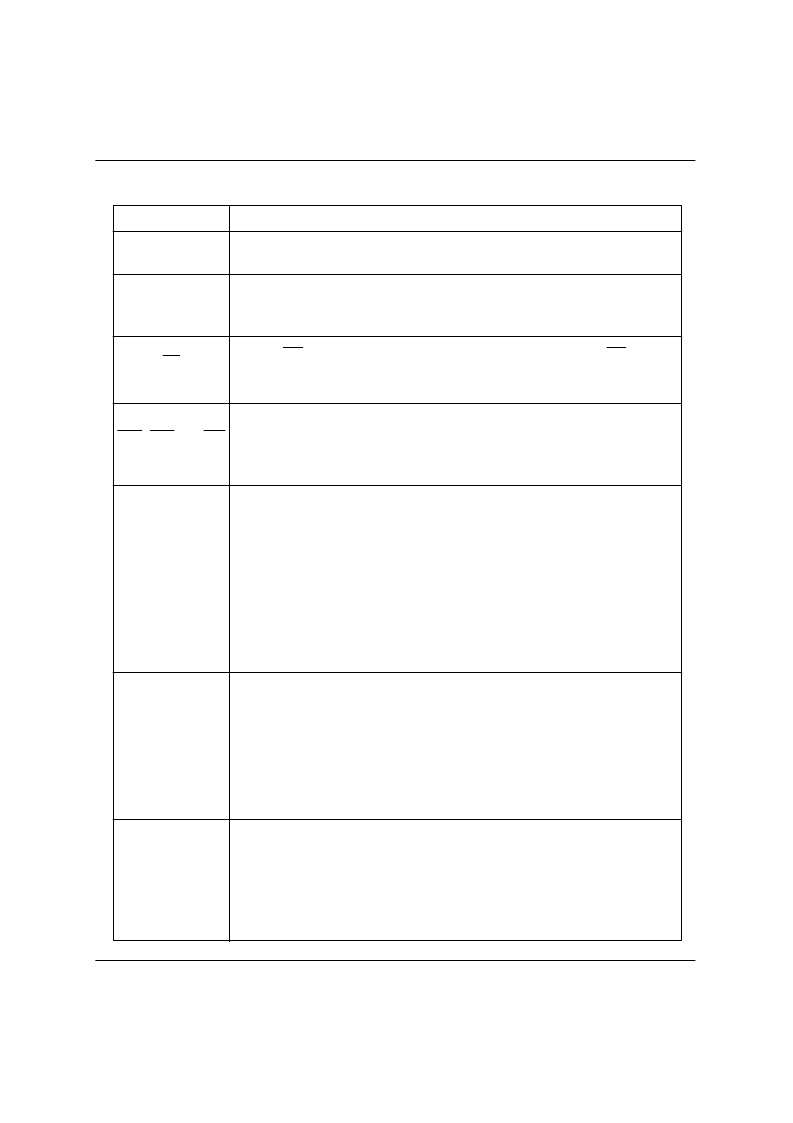
Pin Description
Pin Name
DESCRIPTION
CLK
(input pin)
CLK is the master Clock input to this pin. The other input signals are referred
at CLK rising edge.
CKE
(input pin)
This pin determines whether or not the next CLK is valid. If CKE is High, the
next CLK rising edge is valid. If CKE is Low, the next CLK rising edge is
invalid. This pin is used for Power-down and Clock suspend modes.
CS
(input pin)
When CS is Low, the command input cycle becomes valid. When CS is high,
all inputs are ignored. However, internal operations (bank active, burst
operations, etc.) are held.
Although these pin names are the same as those of conventional DRAMs,
they function in a different way. These pins define operation commands (read,
write, etc.) depending on the combination of their voltage levels. For details,
refer to the command operation section.
RAS, CAS, and WE
(input pins)
A0 ~ A11
(input pins)
Row address (AX0 to AX11) is determined by A0 to A11 level at the bank
active command cycle CLK rising edge. Column address(AY0 to AY8;
GM72V66841CT/CLT) is determined by A0 to A8 level at the read or write
command cycle CLK rising edge. And this column address becomes burst
access start address. A10 defines the Precharge mode. When A10 = High at
the Precharge command cycle, all banks are Precharged. But when A10 =
Low at the Precharge command cycle, only the bank that is selected by
A12/A13 (BS) is Precharged.
A12/A13
(input pin)
A12/A13 are bank select signal (BS). The memory array of the
GM72V66841CT/CLT is divided into bank 0, bank 1, bank2 and bank 3.
GM72V66841CT/CLT contain 4096-row x 512-column x 8-bits. If A12 is
Low and if A13 is Low, bank 0 is selected. If A12 is High and A13 is Low,
bank 1 is selected. If A12 is Low and A13 is High, bank 2 is selected. If A12
is High and A13 is High, bank 3 is selected.
DQM,
DQMU/DQML
(input pins)
DQM, DQMU/DQML controls input/output buffers.
* Read operation: If DQM, DQMU/DQML is High, The output buffer
becomes High-Z. If the DQM, DQMU/DQML is Low, the output buffer
becomes Low-Z.
* Write operation: If DQM, DQMU/DQML is High, the previous data is held
(the new data is not written). If DQM, DQMU/DQML is Low, the data is
written.
3
相关PDF资料 |
PDF描述 |
|---|---|
| GM7630 | FIXED MULTI - OUTPUT REGULATOR |
| GM7630SIP10T | FIXED MULTI - OUTPUT REGULATOR |
| GM76C28A | 2,048 WORDS X 8 BIT CMOS STATIC RAM |
| GM82C803C | 2.88 MB FDC/ DUAL UARTS WITH FIFO PIO / IDE INTERFACE / S-IR/ PNP |
| GMA7496L | 2W+2W AMPLIFIER WITH DC VOLUME CONTROL |
相关代理商/技术参数 |
参数描述 |
|---|---|
| GM72V66841ET-8 | 制造商:未知厂家 制造商全称:未知厂家 功能描述:x8 SDRAM |
| GM72V66841EXX | 制造商:HYNIX 制造商全称:Hynix Semiconductor 功能描述:2,097,152 WORD x 8 BIT x 4 BANK SYNCHRONOUS DYNAMIC RAM |
| GM73V1892H16C | 制造商:Hynix Semi 功能描述: 制造商:LGS 功能描述:73V1892H16C |
| GM74 | 制造商:3M Electronic Products Division 功能描述:Gasket sealing 50ml |
| GM7500 | 制造商:GAMMA 制造商全称:GAMMA 功能描述:PULSE-WIDTH-MODULATION CONTROL CIRCUITS |
发布紧急采购,3分钟左右您将得到回复。