- 您现在的位置:买卖IC网 > PDF目录383015 > GS7025-CQM (Electronic Theatre Controls, Inc.) Serial Digital Receiver PDF资料下载
参数资料
| 型号: | GS7025-CQM |
| 厂商: | Electronic Theatre Controls, Inc. |
| 英文描述: | Serial Digital Receiver |
| 中文描述: | 串行数字接收机 |
| 文件页数: | 9/13页 |
| 文件大小: | 134K |
| 代理商: | GS7025-CQM |
GENNUM CORPORATION
522 - 80 - 00
9
G
provides a 100mVp-p
signal when driving a 50
oscilloscope input. Due to additional power consumed by
this diagnostic circuit, it is not recommended for continuous
operation.
2. RECLOCKER
The reclocker receives a differential serial data stream from
the internal multiplexer. It locks an internal clock to the
incoming data. It outputs the differential PECL retimed data
signal on SDO/SDO. It outputs the recovered clock on SCO/
SCO. The timing between the output and clock signals is
shown in Figure 9.
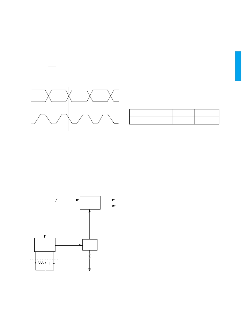
Fig. 9 Output and Clock Signal Timing
The reclocker contains three main functional blocks: the
Phase Locked Loop, Frequency Acquisition, and Logic
Circuit.
2-1. Phase Locked Loop (PLL)
The Phase Locked Loop locks the internal PLL clock to the
incoming data rate. A simplified block diagram of the PLL is
shown below. The main components are the VCO, the
phase detector, the charge pump, and the loop filter.
Fig. 10 Simplified Block Diagram of the PLL
2-2. VCO
The VCO is a differential low phase noise, factory trimmed
oscillator that provides increased immunity to PCB noise
and precise control of the VCO centre frequency. The VCO
has a pull range of ±15% about the centre frequency. A
single low impedance external resistor, R
VCO
, sets the VCO
centre frequency. The low impedance R
VCO
minimizes
thermal noise and reduces the PLL's sensitivity to PCB
noise.
The recommended R
VCO
value for SMPTE 259M-C
applications is 365
.
When the input data stream is removed for an excessive
period of time (see AC electrical characteristics table),the
VCO frequency can drift from the 270Mb/s centre frequency
to the limits shown in Table1.
2-3. Phase Detector
The phase detector compares the phase of the PLL clock
with the phase of the incoming data signal and generates
error correcting timing pulses. The phase detector design
provides a linear transfer function which maximizes the
input jitter tolerance of the PLL.
2-4. Charge Pump
The charge pump takes the phase detector output timing
pulses and creates a charge packet that is proportional to
the system phase error. A unique differential charge pump
design insures that the output phase does not drift when
data transitions are sparse. This makes the GS7025 ideal
for SMPTE 259M-C applications where pathological signals
have data transition densities of 0.05.
2-5. Loop Filter
The loop filter integrates the charge pump packets and
produces a VCO control voltage. The loop filter is
comprised of three external components which are
connected to pins LF+, LFS, and LF-. The loop filter design
is fully differential giving the GS7025 increased immunity to
PCB board noise.
The loop filter components are critical in determining the
loop bandwidth and damping of the PLL. Choosing these
component values is discussed in detail in the PLL DESIGN
GUIDELINES section. Recommended values for SMPTE
259M-C applications are shown in the Typical Application
Circuit. No further changes from the recommended GS7025
loop filter components are necessary.
SDO
SCO
50%
DDI/DDI
LF+
LFS
LF-
R
VCO
VCO
R
LF
C
LF1
C
LF2
2
PHASE
DETECTOR
INTERNAL
PLL CLOCK
CHARGE
PUMP
LOOP
FILTER
TABLE 1: Frequency Drift Range
FREQUENCY
MIN (%)
MAX(%)
270Mb/s lock
-13
28
相关PDF资料 |
PDF描述 |
|---|---|
| GS7025-CTM | Serial Digital Receiver |
| GS702 | Flexible Remote Control (FRC) Technology ? Transmitter |
| GS70328SJ-10IT | 32K x 8 256Kb Asynchronous SRAM |
| GS70328SJ-10T | 32K x 8 256Kb Asynchronous SRAM |
| GS70328SJ-12IT | 32K x 8 256Kb Asynchronous SRAM |
相关代理商/技术参数 |
参数描述 |
|---|---|
| GS7025-CQME3 | 制造商:Semtech Corporation 功能描述:Serial Digital Receiver 44-Pin MQFP Tray 制造商:Semtech Corporation 功能描述:270 Mb/s Receiver |
| GS7025-CTM | 制造商:GENNUM 制造商全称:GENNUM 功能描述:Serial Digital Receiver |
| GS7032 | 制造商:未知厂家 制造商全称:未知厂家 功能描述:32K x 8 256Kb Asynchronous SRAM |
| GS70328GJ-12 | 制造商:GSI Technology 功能描述: |
| GS70328GS-10 | 制造商:GSI Technology 功能描述:32K X 8 (256K) FAST ASYNCH SRAM 3.3V - Trays |
发布紧急采购,3分钟左右您将得到回复。