- 您现在的位置:买卖IC网 > PDF目录296050 > GS8182S18BD-300IT (GSI TECHNOLOGY) 1M X 18 DDR SRAM, 0.45 ns, PBGA165 PDF资料下载
参数资料
| 型号: | GS8182S18BD-300IT |
| 厂商: | GSI TECHNOLOGY |
| 元件分类: | SRAM |
| 英文描述: | 1M X 18 DDR SRAM, 0.45 ns, PBGA165 |
| 封装: | 13 X 15 MM, 1 MM PITCH, FPBGA-165 |
| 文件页数: | 1/37页 |
| 文件大小: | 564K |
| 代理商: | GS8182S18BD-300IT |
当前第1页第2页第3页第4页第5页第6页第7页第8页第9页第10页第11页第12页第13页第14页第15页第16页第17页第18页第19页第20页第21页第22页第23页第24页第25页第26页第27页第28页第29页第30页第31页第32页第33页第34页第35页第36页第37页
GS8182S08/09/18/36BD-400/375/333/300/250/200/167
18Mb Burst of 2
SigmaSIO DDR-IITM SRAM
400 MHz–167 MHz
1.8 V VDD
1.8 V and 1.5 V I/O
165-Bump BGA
Commercial Temp
Industrial Temp
Rev: 1.03b 6/2010
1/37
2007, GSI Technology
Specifications cited are subject to change without notice. For latest documentation see http://www.gsitechnology.com.
Features
Simultaneous Read and Write SigmaSIO Interface
JEDEC-standard pinout and package
Dual Double Data Rate interface
Byte Write controls sampled at data-in time
DLL circuitry for wide output data valid window and future
frequency scaling
Burst of 2 Read and Write
1.8 V +100/–100 mV core power supply
1.5 V or 1.8 V HSTL Interface
Pipelined read operation
Fully coherent read and write pipelines
ZQ mode pin for programmable output drive strength
IEEE 1149.1 JTAG-compliant Boundary Scan
Pin-compatible with present 9Mb, 36Mb, and 72Mb and
future 144Mb devices
165-bump, 13 mm x 15 mm, 1 mm bump pitch BGA package
RoHS-compliant 165-bump BGA package available
SigmaSIO DDR-II Family Overview
GS8182S08/09/18/36BD are built in compliance with the
SigmaSIO DDR-II SRAM pinout standard for Separate I/O
synchronous SRAMs. They are 18,874,368-bit (18Mb)
SRAMs. These are the first in a family of wide, very low
voltage HSTL I/O SRAMs designed to operate at the speeds
needed to implement economical high performance
networking systems.
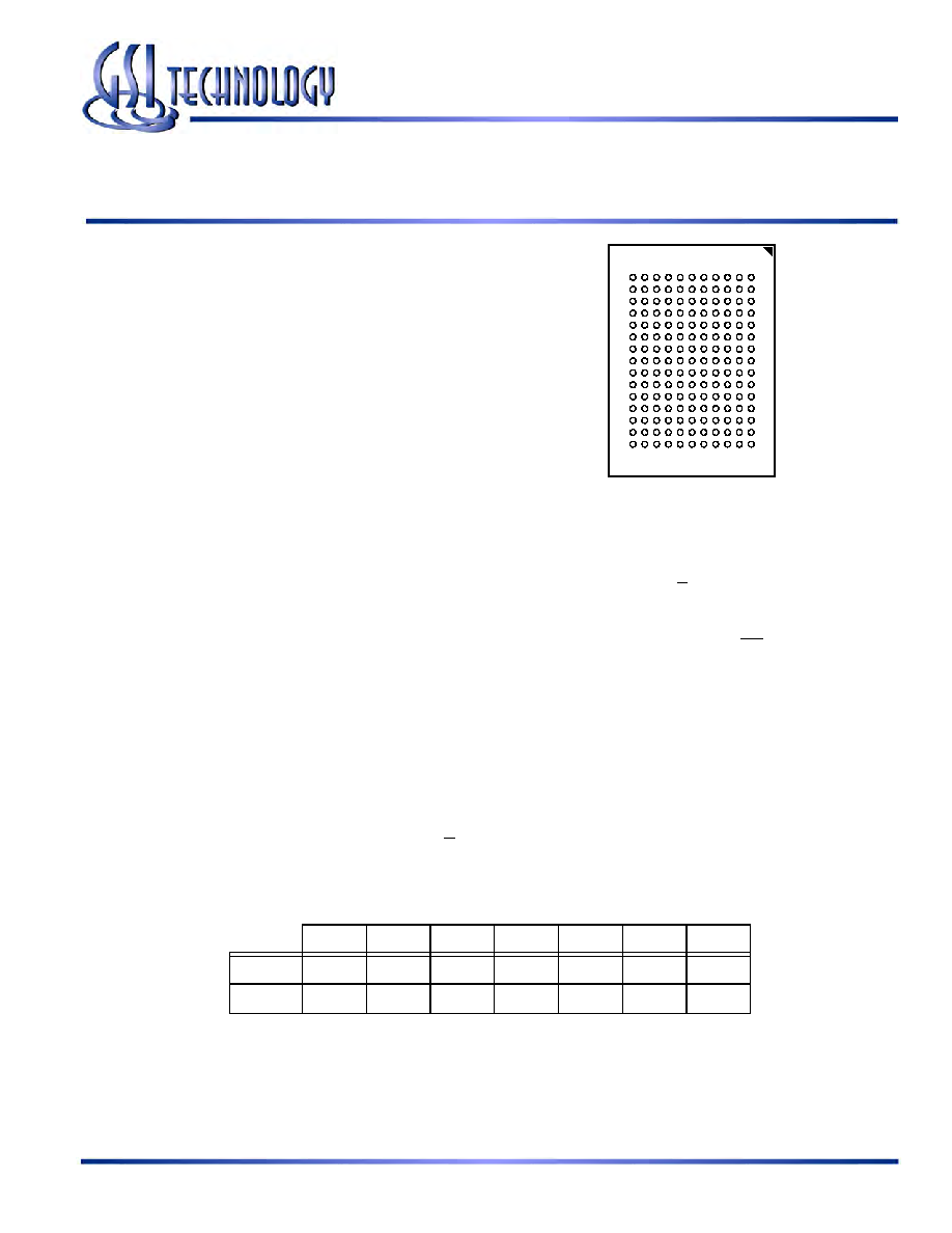
165-Bump, 13 mm x 15 mm BGA
1 mm Bump Pitch, 11 x 15 Bump Array
Bottom View
JEDEC Std. MO-216, Variation CAB-1
Clocking and Addressing Schemes
A Burst of 2 SigmaSIO DDR-II SRAM is a synchronous
device. It employs dual input register clock inputs, K and K.
The device also allows the user to manipulate the output
register clock input quasi independently with dual output
register clock inputs, C and C. If the C clocks are tied high, the
K clocks are routed internally to fire the output registers
instead. Each Burst of 2 SigmaSIO DDR-II SRAM also
supplies Echo Clock outputs, CQ and CQ, which are
synchronized with read data output. When used in a source
synchronous clocking scheme, the Echo Clock outputs can be
used to fire input registers at the data’s destination.
Because Separate I/O Burst of 2 RAMs always transfer data in
two packets, A0 is internally set to 0 for the first read or write
transfer, and automatically incremented by 1 for the next
transfer. Because the LSB is tied off internally, the address
field of a Burst of 2 RAM is always one address pin less than
the advertised index depth (e.g., the 1M x 18 has a 512K
addressable index).
Parameter Synopsis
-400
-375
-333
-300
-250
-200
-167
tKHKH
2.5 ns
2.67 ns
3.0 ns
3.3 ns
4.0 ns
5.0 ns
6.0 ns
tKHQV
0.45 ns
0.5 ns
相关PDF资料 |
PDF描述 |
|---|---|
| GS8182S18BD-250I | 1M X 18 DDR SRAM, 0.45 ns, PBGA165 |
| GS8182S18BD-300I | 1M X 18 DDR SRAM, 0.45 ns, PBGA165 |
| GS8182T08GBD-167IT | 2M X 8 DDR SRAM, 0.5 ns, PBGA165 |
| GS82032AT-4I | 64K X 32 CACHE SRAM, 10 ns, PQFP100 |
| GS8342S36AE-200S | 1M X 36 DDR SRAM, 0.45 ns, PBGA165 |
相关代理商/技术参数 |
参数描述 |
|---|---|
| GS8182S18D-250 | 制造商:GSI Technology 功能描述:SRAM SYNC DUAL 1.8V 18MBIT 1MX18 0.45NS 165FBGA - Trays |
| GS8182S18D-250I | 制造商:GSI Technology 功能描述:SRAM SYNC DUAL 1.8V 18MBIT 1MX18 0.45NS 165FPBGA - Trays |
| GS8182S36BD-167 | 制造商:GSI Technology 功能描述:512K X 36 (18 MEG) BURST OF 2 - Trays |
| GS8182S36BD-167I | 制造商:GSI Technology 功能描述:512K X 36 (18 MEG) BURST OF 2 - Trays |
| GS8182S36BD-200 | 制造商:GSI Technology 功能描述:512K X 36 (18 MEG) BURST OF 2 - Trays |
发布紧急采购,3分钟左右您将得到回复。