- 您现在的位置:买卖IC网 > PDF目录385320 > GS8322ZV18B-150I (GSI TECHNOLOGY) 36Mb Pipelined and Flow Through Synchronous NBT SRAM PDF资料下载
参数资料
| 型号: | GS8322ZV18B-150I |
| 厂商: | GSI TECHNOLOGY |
| 元件分类: | DRAM |
| 英文描述: | 36Mb Pipelined and Flow Through Synchronous NBT SRAM |
| 中文描述: | 2M X 18 ZBT SRAM, 8.5 ns, PBGA119 |
| 封装: | 14 X 22 MM, 1.27 PITCH, FPBGA-119 |
| 文件页数: | 12/39页 |
| 文件大小: | 975K |
| 代理商: | GS8322ZV18B-150I |
第1页第2页第3页第4页第5页第6页第7页第8页第9页第10页第11页当前第12页第13页第14页第15页第16页第17页第18页第19页第20页第21页第22页第23页第24页第25页第26页第27页第28页第29页第30页第31页第32页第33页第34页第35页第36页第37页第38页第39页
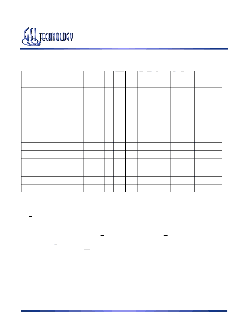
Synchronous Truth Table
Operation
Type
Address
CK CKE ADV W Bx E
1
E
2
E
3
G ZZ
DQ
Notes
Read Cycle, Begin Burst
R
External
L-H
L
L
H
X
L
H
L
L
L
Q
Read Cycle, Continue Burst
B
Next
L-H
L
H
X
X
X
X
X
L
L
Q
1,10
NOP/Read, Begin Burst
R
External
L-H
L
L
H
X
L
H
L
H
L
High-Z
2
Dummy Read, Continue Burst
B
Next
L-H
L
H
X
X
X
X
X
H
L
High-Z
1,2,10
Write Cycle, Begin Burst
W
External
L-H
L
L
L
L
L
H
L
X
L
D
3
Write Cycle, Continue Burst
B
Next
L-H
L
H
X
L
X
X
X
X
L
D
1,3,10
Write Abort, Continue Burst
B
Next
L-H
L
H
X
H
X
X
X
X
L
High-Z 1,2,3,10
Deselect Cycle, Power Down
D
None
L-H
L
L
X
X
H
X
X
X
L
High-Z
Deselect Cycle, Power Down
D
None
L-H
L
L
X
X
X
X
H
X
L
High-Z
Deselect Cycle, Power Down
D
None
L-H
L
L
X
X
X
L
X
X
L
High-Z
Deselect Cycle
D
None
L-H
L
L
L
H
L
H
L
X
L
High-Z
1
Deselect Cycle, Continue
D
None
L-H
L
H
X
X
X
X
X
X
L
High-Z
1
Sleep Mode
None
X
X
X
X
X
X
X
X
X
H
High-Z
Clock Edge Ignore, Stall
Current
L-H
H
X
X
X
X
X
X
X
L
-
4
Notes:
1.
Continue Burst cycles, whether read or write, use the same control inputs. A Deselect continue cycle can only be entered into if a Dese-
lect cycle is executed first.
Dummy Read and Write abort can be considered NOPs because the SRAM performs no operation. A Write abort occurs when the W
pin is sampled low but no Byte Write pins are active so no write operation is performed.
G can be wired low to minimize the number of control signals provided to the SRAM. Output drivers will automatically turn off during
write cycles.
If CKE High occurs during a pipelined read cycle, the DQ bus will remain active (Low Z). If CKE High occurs during a write cycle, the bus
will remain in High Z.
X = Don’t Care; H = Logic High; L = Logic Low; Bx = High = All Byte Write signals are high; Bx = Low = One or more Byte/Write
signals are Low
All inputs, except G and ZZ must meet setup and hold times of rising clock edge.
Wait states can be inserted by setting CKE high.
This device contains circuitry that ensures all outputs are in High Z during power-up.
A 2-bit burst counter is incorporated.
10. The address counter is incriminated for all Burst continue cycles.
2.
3.
4.
5.
6.
7.
8.
9.
GS8322ZV18(B/E)/GS8322ZV36(B/E)/GS8322ZV72(C)
Specifications cited are subject to change without notice. For latest documentation see http://www.gsitechnology.com.
Rev: 1.03a 2/2006
12/39
2002, GSI Technology
相关PDF资料 |
PDF描述 |
|---|---|
| GS8322ZV18B-166 | 36Mb Pipelined and Flow Through Synchronous NBT SRAM |
| GS8322ZV18B-166I | 36Mb Pipelined and Flow Through Synchronous NBT SRAM |
| GS8322ZV18B-200 | 36Mb Pipelined and Flow Through Synchronous NBT SRAM |
| GS8322ZV18B-200I | 36Mb Pipelined and Flow Through Synchronous NBT SRAM |
| GS8322ZV18B-225 | 36Mb Pipelined and Flow Through Synchronous NBT SRAM |
相关代理商/技术参数 |
参数描述 |
|---|---|
| GS8322ZV72C-133 | 制造商:GSI Technology 功能描述:SRAM SYNC OCTAL 1.8V 36MBIT 512KX72 8.5NS/4NS 209FBGA - Trays |
| GS8322ZV72C-150 | 制造商:GSI Technology 功能描述:SRAM SYNC OCTAL 1.8V 36MBIT 512KX72 8.5NS/3.8NS 209FBGA - Trays |
| GS8322ZV72C-166 | 制造商:GSI Technology 功能描述:SRAM SYNC OCTAL 1.8V 36MBIT 512KX72 8NS/3.5NS 209FBGA - Trays |
| GS8324Z36B-133 | 制造商:GSI Technology 功能描述:SRAM SYNC QUAD 2.5V/3.3V 36MBIT 1MX36 10NS/4NS 119FBGA - Trays |
| GS8324Z36B-200I | 制造商:GSI Technology 功能描述:SRAM SYNC QUAD 2.5V/3.3V 36MBIT 1MX36 7.5NS/3NS 119FBGA - Trays |
发布紧急采购,3分钟左右您将得到回复。