- 您现在的位置:买卖IC网 > PDF目录385327 > GS8640Z36GT-200IV (GSI TECHNOLOGY) 72Mb Pipelined and Flow Through Synchronous NBT SRAM PDF资料下载
参数资料
| 型号: | GS8640Z36GT-200IV |
| 厂商: | GSI TECHNOLOGY |
| 元件分类: | DRAM |
| 英文描述: | 72Mb Pipelined and Flow Through Synchronous NBT SRAM |
| 中文描述: | 2M X 36 ZBT SRAM, 7.5 ns, PQFP100 |
| 封装: | ROHS COMPLIANT, TQFP-100 |
| 文件页数: | 11/22页 |
| 文件大小: | 600K |
| 代理商: | GS8640Z36GT-200IV |
GS8640Z18/36T-xxxV
Preliminary
Specifications cited are subject to change without notice. For latest documentation see http://www.gsitechnology.com.
Rev: 1.01 6/2006
11/22
2004, GSI Technology
Burst Cycles
Although NBT RAMs are designed to sustain 100% bus bandwidth by eliminating turnaround cycle when there is transition from
read to write, multiple back-to-back reads or writes may also be performed. NBT SRAMs provide an on-chip burst address
generator that can be utilized, if desired, to further simplify burst read or write implementations. The ADV control pin, when
driven high, commands the SRAM to advance the internal address counter and use the counter generated address to read or write
the SRAM. The starting address for the first cycle in a burst cycle series is loaded into the SRAM by driving the ADV pin low, into
Load mode.
Burst Order
The burst address counter wraps around to its initial state after four addresses (the loaded address and three more) have been
accessed. The burst sequence is determined by the state of the Linear Burst Order pin (LBO). When this pin is low, a linear burst
sequence is selected. When the RAM is installed with the LBO pin tied high, Interleaved burst sequence is selected. See the tables
below for details.
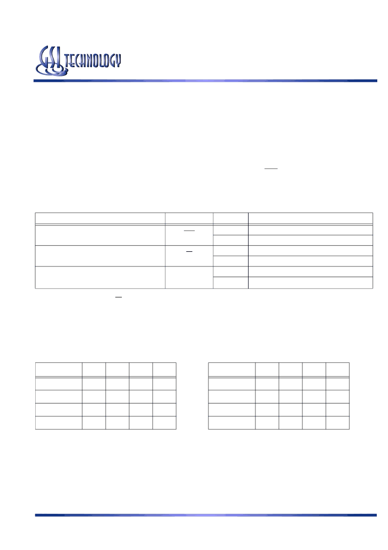
Mode Pin Functions
Mode Name
Pin Name
State
L
H
L
H or NC
L or NC
Function
Linear Burst
Interleaved Burst
Flow Through
Pipeline
Active
Standby, I
DD
= I
SB
Burst Order Control
LBO
Output Register Control
FT
Power Down Control
ZZ
H
Note:
There is a pull-up device on the FT pin and a pull-down device on the ZZ pin, so this input pin can be unconnected and the chip will operate in
the default states as specified in the above table.
Note:
The burst counter wraps to initial state on the 5th clock.
Note:
The burst counter wraps to initial state on the 5th clock.
Linear Burst Sequence
A[1:0] A[1:0] A[1:0] A[1:0]
1st address
00
01
10
11
2nd address
01
10
11
00
3rd address
10
11
00
01
4th address
11
00
01
10
Interleaved Burst Sequence
A[1:0] A[1:0] A[1:0] A[1:0]
1st address
00
01
10
11
2nd address
01
00
11
10
3rd address
10
11
00
01
4th address
11
10
01
00
Burst Counter Sequences
BPR 1999.05.18
相关PDF资料 |
PDF描述 |
|---|---|
| GS8640Z36GT-200V | 72Mb Pipelined and Flow Through Synchronous NBT SRAM |
| GS8640Z36GT-250IV | 72Mb Pipelined and Flow Through Synchronous NBT SRAM |
| GS8640Z36GT-250V | 72Mb Pipelined and Flow Through Synchronous NBT SRAM |
| GS8640Z36T-167IV | 72Mb Pipelined and Flow Through Synchronous NBT SRAM |
| GS8640Z36T-200IV | 72Mb Pipelined and Flow Through Synchronous NBT SRAM |
相关代理商/技术参数 |
参数描述 |
|---|---|
| GS8640Z36GT-200V | 制造商:GSI Technology 功能描述:SRAM SYNC QUAD 1.8V/2.5V 72MBIT 2MX36 7.5NS/3NS 100TQFP - Trays |
| GS8640Z36GT-250 | 制造商:GSI Technology 功能描述:SRAM SYNC QUAD 2.5V/3.3V 72MBIT 2MX36 6.5NS/2.5NS 100TQFP - Trays |
| GS8640Z36GT-250IV | 制造商:GSI Technology 功能描述:SRAM SYNC QUAD 1.8V/2.5V 72MBIT 2MX36 6.5NS/3NS 100TQFP - Trays |
| GS8640Z36GT-250V | 制造商:GSI Technology 功能描述:SRAM SYNC QUAD 1.8V/2.5V 72MBIT 2MX36 6.5NS/3NS 100TQFP - Trays |
| GS8640Z36GT-300 | 制造商:GSI 制造商全称:GSI Technology 功能描述:72Mb Pipelined and Flow Through Synchronous NBT SRAM |
发布紧急采购,3分钟左右您将得到回复。