- 您现在的位置:买卖IC网 > PDF目录385337 > GS8662R09E-167 (GSI TECHNOLOGY) 72Mb SigmaCIO DDR-II Burst of 4 SRAM PDF资料下载
参数资料
| 型号: | GS8662R09E-167 |
| 厂商: | GSI TECHNOLOGY |
| 元件分类: | DRAM |
| 英文描述: | 72Mb SigmaCIO DDR-II Burst of 4 SRAM |
| 中文描述: | 8M X 9 DDR SRAM, 0.5 ns, PBGA165 |
| 封装: | 15 MM X 17 MM, 1MM PITCH, FPBGA-165 |
| 文件页数: | 1/37页 |
| 文件大小: | 942K |
| 代理商: | GS8662R09E-167 |
当前第1页第2页第3页第4页第5页第6页第7页第8页第9页第10页第11页第12页第13页第14页第15页第16页第17页第18页第19页第20页第21页第22页第23页第24页第25页第26页第27页第28页第29页第30页第31页第32页第33页第34页第35页第36页第37页
Preliminary
GS8662R08/09/18/36E-333/300/250/200/167
72Mb SigmaCIO DDR-II
Burst of 4 SRAM
333 MHz–167 MHz
1.8 V V
DD
1.8 V and 1.5 V I/O
165-Bump BGA
Commercial Temp
Industrial Temp
Rev: 1.01 9/2005
Specifications cited are subject to change without notice. For latest documentation see http://www.gsitechnology.com.
1/37
2005, GSI Technology
Features
Simultaneous Read and Write SigmaCIO Interface
Common I/O bus
JEDEC-standard pinout and package
Double Data Rate interface
Byte Write (x36 and x18) and Nybble Write (x8) function
Burst of 4 Read and Write
1.8 V +100/–100 mV core power supply
1.5 V or 1.8 V HSTL Interface
Pipelined read operation with self-timed Late Write
Fully coherent read and write pipelines
ZQ pin for programmable output drive strength
IEEE 1149.1 JTAG-compliant Boundary Scan
Pin-compatible with present 9Mb, 18Mb, 36Mb and future
144Mb devices
165-bump, 15 mm x 17 mm, 1 mm bump pitch BGA package
RoHS-compliant 165-bump BGA package available
SigmaCIO
Family Overview
The GS8662R08/09/18/36E are built in compliance with the
SigmaCIO DDR-II SRAM pinout standard for Common I/O
synchronous SRAMs. They are 75,497,472-bit (72Mb)
SRAMs. The GS8662R08/09/18/36E SigmaCIO SRAMs are
just one element in a family of low power, low voltage HSTL
I/O SRAMs designed to operate at the speeds needed to
implement economical high performance networking systems.
Clocking and Addressing Schemes
The GS8662R08/09/18/36E SigmaCIO DDR-II SRAMs are
synchronous devices. They employ two input register clock
inputs, K and K. K and K are independent single-ended clock
inputs, not differential inputs to a single differential clock input
buffer. The device also allows the user to manipulate the
output register clock inputs quasi independently with the C and
C clock inputs. C and C are also independent single-ended
clock inputs, not differential inputs. If the C clocks are tied
high, the K clocks are routed internally to fire the output
registers instead.
Common I/O x36 and x18 SigmaCIO DDR-II B4
RAMs
always transfer data in four packets. When a new address is
loaded, A0 and A1 preset an internal 2 bit linear address
counter. The counter increments by 1 for each beat of a burst of
four data transfer. The counter always wraps to 00 after
reaching 11, no matter where it starts.
Common I/O x8 SigmaCIO DDR-II B4 RAMs always transfer
data in four packets. When a new address is loaded, the LSBs
are internally set to 0 for the first read or write transfer, and
incremented by 1 for the next 3 transfers. Because the LSBs
are tied off internally, the address field of a x8 SigmaCIO
DDR-II B4 RAM is always two address pins less than the
advertised index depth (e.g., the 4M x 18 has a 1024K
addressable index).
Parameter Synopsis
-333
-300
-250
-200
-167
tKHKH
3.0 ns
3.3 ns
4.0 ns
5.0 ns
6.0 ns
tKHQV
0.45 ns
0.45 ns
0.45 ns
0.45 ns
0.5 ns
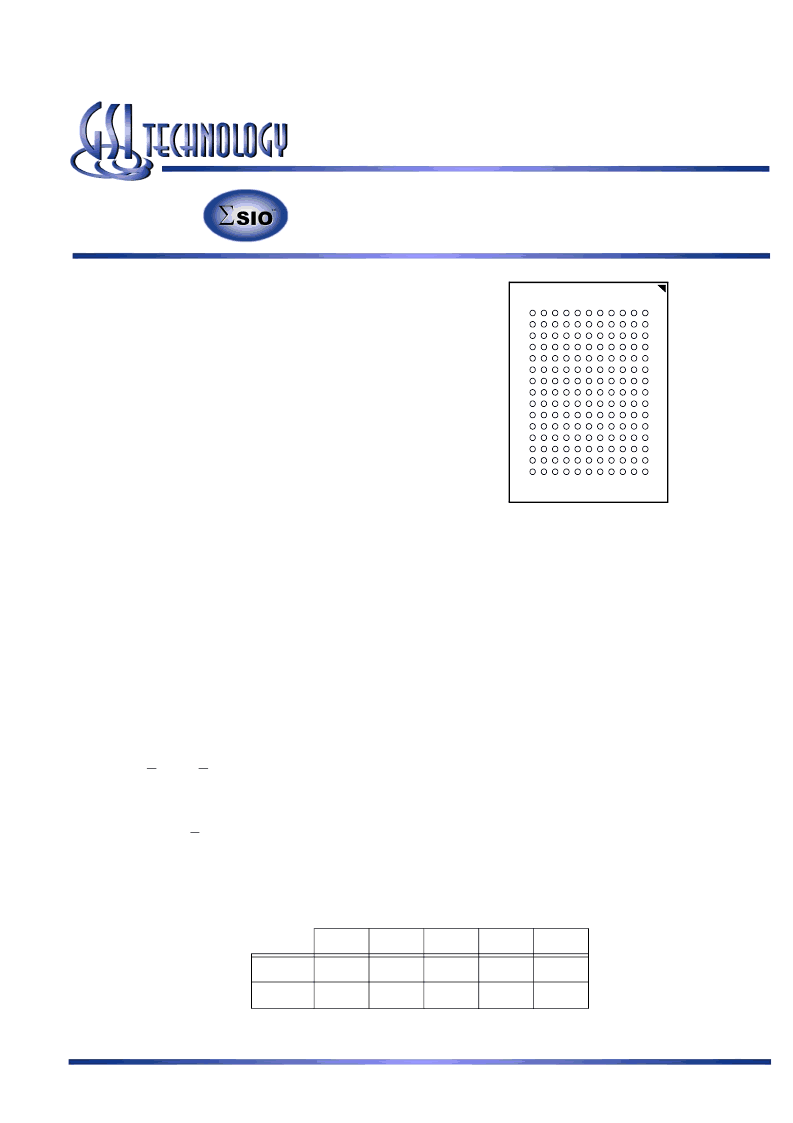
165-Bump, 15 mm x 17 mm BGA
1 mm Bump Pitch, 11 x 15 Bump Array
Bottom View
相关PDF资料 |
PDF描述 |
|---|---|
| GS8662R09E-167I | 72Mb SigmaCIO DDR-II Burst of 4 SRAM |
| GS8662R09E-200 | 72Mb SigmaCIO DDR-II Burst of 4 SRAM |
| GS8662R09E-200I | 72Mb SigmaCIO DDR-II Burst of 4 SRAM |
| GS8662R09E-250 | 72Mb SigmaCIO DDR-II Burst of 4 SRAM |
| GS8662R09E-250I | 72Mb SigmaCIO DDR-II Burst of 4 SRAM |
相关代理商/技术参数 |
参数描述 |
|---|---|
| GS8662R09E-167I | 制造商:GSI 制造商全称:GSI Technology 功能描述:72Mb SigmaCIO DDR-II Burst of 4 SRAM |
| GS8662R09E-200 | 制造商:GSI 制造商全称:GSI Technology 功能描述:72Mb SigmaCIO DDR-II Burst of 4 SRAM |
| GS8662R09E-200I | 制造商:GSI 制造商全称:GSI Technology 功能描述:72Mb SigmaCIO DDR-II Burst of 4 SRAM |
| GS8662R09E-250 | 制造商:GSI 制造商全称:GSI Technology 功能描述:72Mb SigmaCIO DDR-II Burst of 4 SRAM |
| GS8662R09E-250I | 制造商:GSI 制造商全称:GSI Technology 功能描述:72Mb SigmaCIO DDR-II Burst of 4 SRAM |
发布紧急采购,3分钟左右您将得到回复。