- 您现在的位置:买卖IC网 > PDF目录385347 > H1106I (Intersil Corporation) 315MHz, Low Power, Video Operational Amplifier with Compensation Pin PDF资料下载
参数资料
| 型号: | H1106I |
| 厂商: | Intersil Corporation |
| 英文描述: | 315MHz, Low Power, Video Operational Amplifier with Compensation Pin |
| 中文描述: | 315MHz的,低功耗,视频运算放大器补偿引脚 |
| 文件页数: | 5/16页 |
| 文件大小: | 616K |
| 代理商: | H1106I |
3-32
Application Information
Optimum Feedback Resistor
All current feedback amplifiers (CFAs) require a feedback
resistor (R
F
) even for unity gain applications, and R
F
in
conjunction with the internal compensation capacitor sets
the dominant pole of the frequency response. Thus the
amplifier’s bandwidth is inversely proportional to R
F
. The
HFA1106 design is optimized for R
F
= 150
at a gain of +1.
Decreasing R
F
decreases stability resulting in excessive
peaking and overshoot - Note: Capacitive feedback causes
the same problems due to the feedback impedance
decrease at higher frequencies. At higher gains, however,
the amplifier is more stable, so R
F
can be decreased in a
trade-off of stability for bandwidth (e.g., R
F
= 100
for
A
V
= +2).
Why Use Externally Compensated Amplifiers
Externally compensated op amps were originally developed
to allow operation at gains below the amplifier’s minimum
stable gain. This enabled development of non-unity gain sta-
ble op amps with very high bandwidth and slew rates. Users
needing lower closed loop gains could stabilize the amplifier
with external compensation if the associated performance
decrease was tolerable.
With the advent of CFAs, unity gain stability and high perfor-
mance are no longer mutually exclusive, so why offer unity
gain stable op amps with compensation pins
The main reason for external compensation is to allow users
to tailor the amplifier’s performance to their specific system
needs. Bandwidth can be limited to the exact value required,
thereby eliminating excess bandwidth and its associated
noise. A compensated op amp is also more predictable;
lower lot-to-lot variation requires less system overdesign to
cover process variability. Finally, access to the internal high
impedance node allows users to implement external output
limiting or allows for stabilizing the amplifier when driving
large capacitive loads.
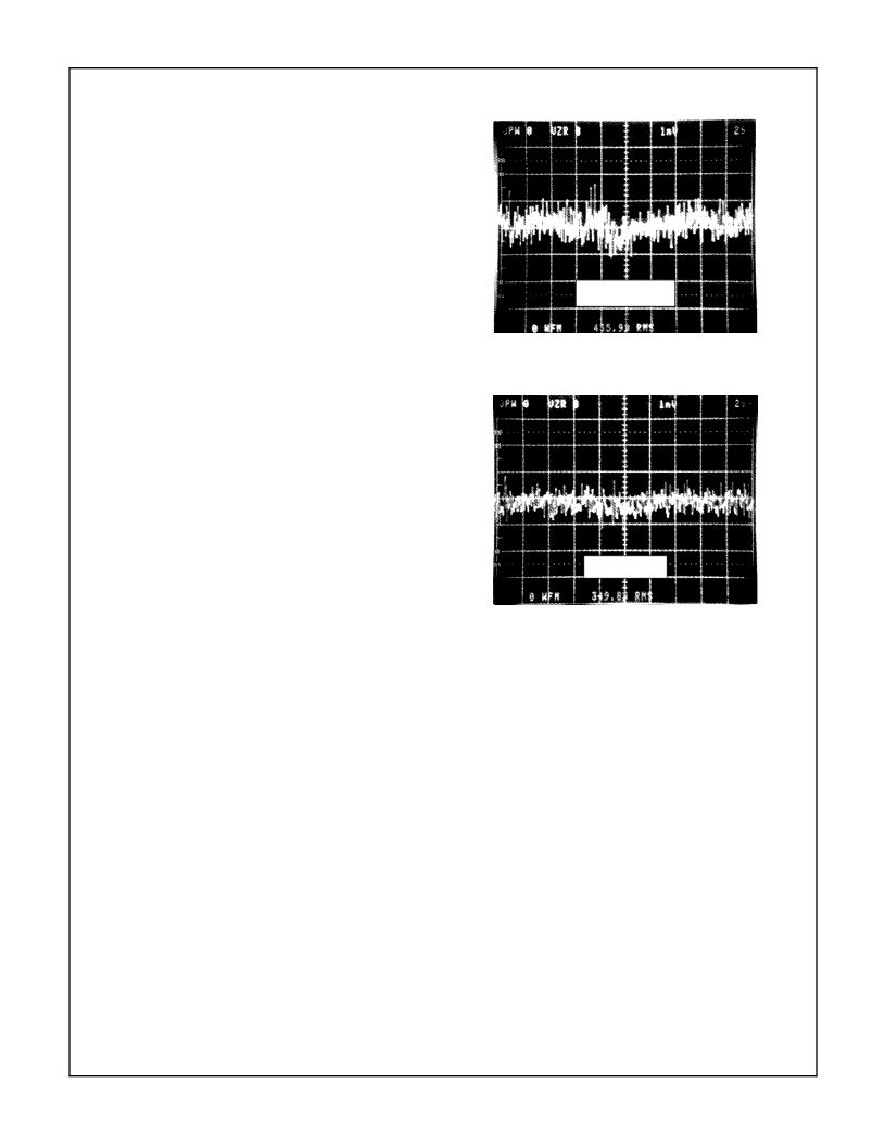
Noise Advantages - Uncompensated
The HFA1106 delivers lower broadband noise even without
an external compensation capacitor. Package capacitance
present at the Comp pin stabilizes the op amp, so lower
value feedback resistors can be used. A smaller value R
F
minimizes the noise voltage contribution of the amplifier’s
inverting input noise current - I
NI
x R
F
, usually a large con-
tributor on CFAs - and minimizes the resistor’s thermal noise
contribution (4KTR
F
). Figure 1 details the HFA1105 broad-
band noise performance in its recommended configuration
of A
V
= +2, and R
F
= 510
. Adding a Comp pin to the
HFA1105 (thereby creating the HFA1106) yields the 23%
noise reduction shown in Figure 2.
In both cases, the scope
bandwidth, 100MHz, limits the measurement range to pre-
vent amplifier bandwidth differences from affecting the
results.
Offset Advantage
An added advantage of the lower value R
F
is a smaller DC
output offset. The op amp’s inverting input bias current (I
BI
)
flows through the feedback resistor and generates an offset
voltage error defined by:
Reducing R
F
reduces these errors.
Bandwidth Limiting
The HFA1106 bandwidth may be limited by connecting a
resistor, R
COMP
(required to damp the interaction between
the compensation capacitor and the package parasitics),
and capacitor, C
COMP
, in series from pin 8 to GND. Typical
performance characteristics for various C
COMP
values are
listed in the specification table. The HFA1106 is already
unity gain stable, so the main reason for limiting the band-
width is to reduce the broadband noise.
Noise Advantages - Compensated
System noise reduction is maximized by limiting the op amp to
the bandwidth required for the application. Noise increases as
the square root of the bandwidth increase (4x bandwidth
increase yields 2x noise increase), so eliminating excess
E
N
= 456
μ
V
RMS
FIGURE 1. HFA1105 NOISE PERFORMANCE, A
V
= +2,
R
F
= 510
E
N
= 350
μ
V
RMS
FIGURE 2. HFA1106 NOISE PERFORMANCE,
UNCOMPENSATED, A
V
= +2, R
F
= 100
V
E
I
BI
x R
F
=
and
;
V
OS
A
V
V
IO
±
(
)
V
E
±
=
HFA1106
相关PDF资料 |
PDF描述 |
|---|---|
| H1114I | 850MHz Video Cable Driving Buffer |
| H11A1X | OPTICALLY COUPLED ISOLATOR PHOTOTRANSISTOR OUTPUT |
| H11A2X | OPTICALLY COUPLED ISOLATOR PHOTOTRANSISTOR OUTPUT |
| H11A3X | OPTICALLY COUPLED ISOLATOR PHOTOTRANSISTOR OUTPUT |
| H11A4X | OPTICALLY COUPLED ISOLATOR PHOTOTRANSISTOR OUTPUT |
相关代理商/技术参数 |
参数描述 |
|---|---|
| H-11-1 | 制造商:Hozan Tool Industrial 功能描述:KReFH-11 |
| H1112 | 功能描述:变压器音频和信号 10/100BASE-TX 1:1 RoHS:否 制造商:Skyworks Solutions, Inc. 频率范围:810 MHz to 960 MHz 初级线圈阻抗: 次级线圈阻抗: 绝缘电压:23 dB 工作温度范围:- 40 C to + 85 C 端接类型:SMD/SMT 尺寸:6 mm L x 4.9 mm W x 1.6 mm H 产品:Splitters and Combiners |
| H1112NL | 功能描述:变压器音频和信号 10/100BASE-TX 1:1 RoHS:否 制造商:Skyworks Solutions, Inc. 频率范围:810 MHz to 960 MHz 初级线圈阻抗: 次级线圈阻抗: 绝缘电压:23 dB 工作温度范围:- 40 C to + 85 C 端接类型:SMD/SMT 尺寸:6 mm L x 4.9 mm W x 1.6 mm H 产品:Splitters and Combiners |
| H1112NLT | 功能描述:变压器音频和信号 10/100BASE-TX 1:1 RoHS:否 制造商:Skyworks Solutions, Inc. 频率范围:810 MHz to 960 MHz 初级线圈阻抗: 次级线圈阻抗: 绝缘电压:23 dB 工作温度范围:- 40 C to + 85 C 端接类型:SMD/SMT 尺寸:6 mm L x 4.9 mm W x 1.6 mm H 产品:Splitters and Combiners |
| H1112T | 功能描述:变压器音频和信号 10/100BASE-TX 1:1 RoHS:否 制造商:Skyworks Solutions, Inc. 频率范围:810 MHz to 960 MHz 初级线圈阻抗: 次级线圈阻抗: 绝缘电压:23 dB 工作温度范围:- 40 C to + 85 C 端接类型:SMD/SMT 尺寸:6 mm L x 4.9 mm W x 1.6 mm H 产品:Splitters and Combiners |
发布紧急采购,3分钟左右您将得到回复。