- 您现在的位置:买卖IC网 > PDF目录385347 > H1114I (Intersil Corporation) 850MHz Video Cable Driving Buffer PDF资料下载
参数资料
| 型号: | H1114I |
| 厂商: | Intersil Corporation |
| 英文描述: | 850MHz Video Cable Driving Buffer |
| 中文描述: | 850MHz的视频线驱动缓冲器 |
| 文件页数: | 4/5页 |
| 文件大小: | 143K |
| 代理商: | H1114I |
4
Application Information
Closed Loop Gain Selection
The HFA1114 features a novel design which allows the user
to select from three closed loop gains, without any external
components. The result is a more flexible product, fewer part
types in inventory, and more efficient use of board space.
This “buffer” operates in closed loop gains of -1, +1, or +2, and
gain selection is accomplished via connections to the
±
inputs.
Applying the input signal to +IN and floating -IN selects a gain
of +1, while grounding -IN selects a gain of +2. A gain of -1 is
obtained by applying the input signal to -IN with +IN grounded.
The table below summarizes these connections:
PC Board Layout
The frequency response of this amplifier depends greatly on
the amount of care taken in designing the PC board.
The
use of low inductance components such as chip resis-
tors and chip capacitors is strongly recommended,
while a solid ground plane is a must!
Attention should be given to decoupling the power supplies.
A large value (10
μ
F) tantalum in parallel with a small value
(0.1
μ
F) chip capacitor works well in most cases.
Terminated microstrip signal lines are recommended at the input
and output of the device. Capacitance directly on the output must
be minimized, or isolated as discussed in the next section.
For unity gain applications, care must also be taken to minimize
the capacitance to ground seen by the amplifier’s inverting
input. At higher frequencies this capacitance will tend to short
the -INPUT to GND, resulting in a closed loop gain which
increases with frequency. This will cause excessive high
frequency peaking and potentially other problems as well.
An example of a good high frequency layout is the Evaluation
Board shown in Figure 2.
Driving Capacitive Loads
Capacitive loads, such as an A/D input, or an improperly
terminated transmission line will degrade the amplifier’s phase
margin resulting in frequency response peaking and possible oscil-
lations. In most cases, the oscillation can be avoided by placing a
resistor (R
S
) in series with the output prior to the capacitance.
Figure 1 details starting points for the selection of this resis-
tor. The points on the curve indicate the R
S
and C
L
combina-
tions for the optimum bandwidth, stability, and settling time,
but experimental fine tuning is recommended. Picking a
point above or to the right of the curve yields an overdamped
response, while points below or left of the curve indicate
areas of underdamped performance.
R
S
and C
L
form a low pass network at the output, thus
limiting system bandwidth well below the amplifier band-
width of 850MHz. By decreasing R
S
as C
L
increases (as
illustrated in the curves), the maximum bandwidth is
obtained without sacrificing stability. Even so, bandwidth
does decrease as you move to the right along the curve.
For example, at A
V
= +1, R
S
= 50
, C
L
= 30pF, the over-
all bandwidth is limited to 300MHz, and bandwidth drops
to 100MHz at A
V
= +1, R
S
= 5
, C
L
= 340pF.
Evaluation Board
The performance of the HFA1114 may be evaluated using
the HFA11XX Evaluation Board, slightly modified as follows:
2. Remove the 500
feedback resistor (R
2
), and leave the
connection open.
3. a. For A
V
= +1 evaluation, remove the 500
gain setting
resistor (R
1
), and leave pin 2 floating.
b. For A
V
= +2, replace the 500
gain setting resistor with
a 0
resistor to GND.
4. Isolate Pin 5 from the stray board capacitance to minimize
peaking and overshoot.
The layout and modified schematic of the board are shown in
Figure 2.
To order evaluation boards (part number HFA11XXEVAL),
please contact your local sales office.
Note: The SOIC version may be evaluated in the DIP board by
using a SOIC-to-DIP adapter such as Aries Electronics Part
Number 08-350000-10.
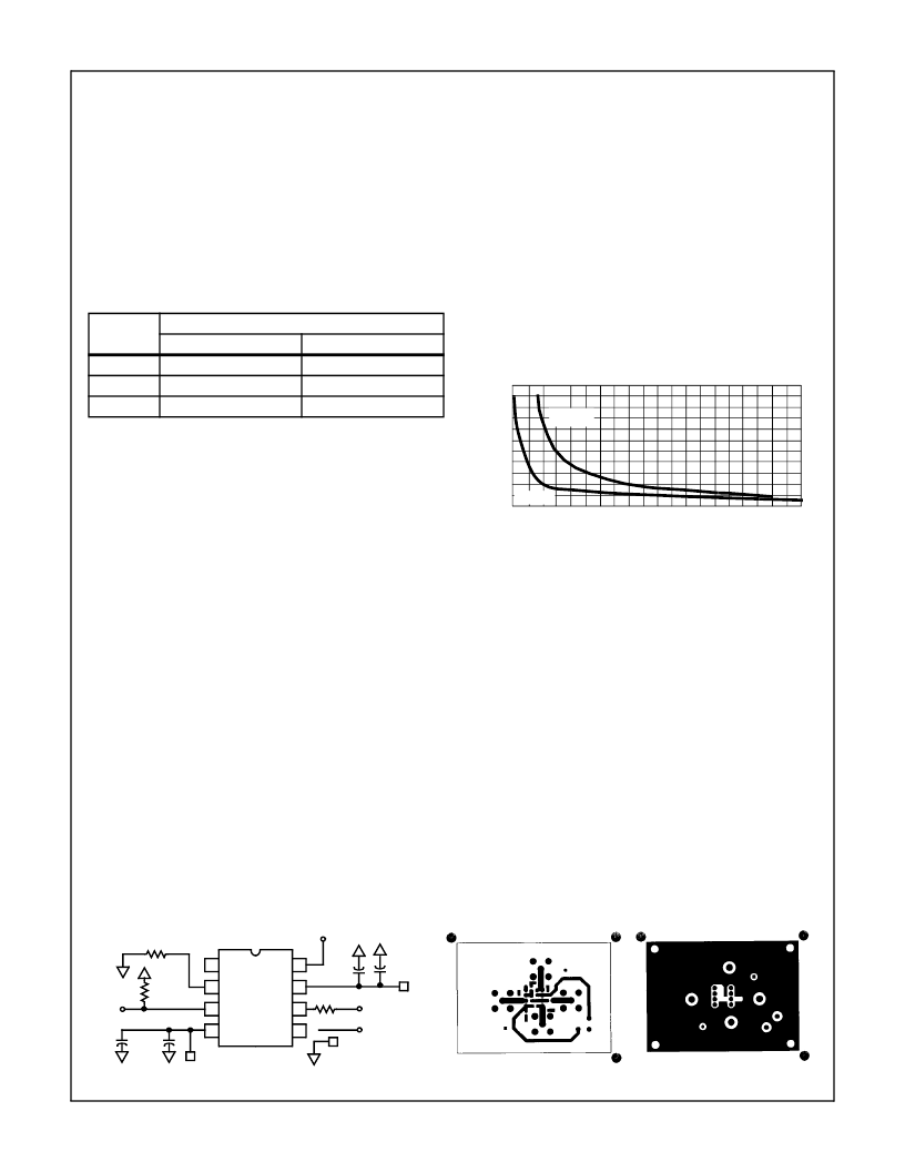
GAIN
(A
CL
)
-1
CONNECTIONS
+INPUT (PIN 3)
-INPUT (PIN 2)
GND
Input
+1
Input
NC (Floating)
+2
Input
GND
R
S
)
LOAD CAPACITANCE (pF)
50
45
40
35
30
25
20
15
10
5
0
0
40
80
120
160
200
240
280
320
360
400
A
V
= +1
A
V
= +2
FIGURE 1. RECOMMENDED SERIES OUTPUT RESISTOR vs
LOAD CAPACITANCE
1
2
3
4
8
7
6
5
+5V
10
μ
F
0.1
μ
F
V
H
50
GND
GND
R
1
-5V
0.1
μ
F
10
μ
F
50
IN
OUT
V
L
∞
(A
V
= +1)
or 0
(A
V
= +2)
V
H
+IN
V
L
V+
GND
1
V-
OUT
TOP LAYOUT
BOTTOM LAYOUT
X
FIGURE 2. EVALUATION BOARD SCHEMATIC AND LAYOUT
HFA1114
相关PDF资料 |
PDF描述 |
|---|---|
| H11A1X | OPTICALLY COUPLED ISOLATOR PHOTOTRANSISTOR OUTPUT |
| H11A2X | OPTICALLY COUPLED ISOLATOR PHOTOTRANSISTOR OUTPUT |
| H11A3X | OPTICALLY COUPLED ISOLATOR PHOTOTRANSISTOR OUTPUT |
| H11A4X | OPTICALLY COUPLED ISOLATOR PHOTOTRANSISTOR OUTPUT |
| H11A5X | OPTICALLY COUPLED ISOLATOR PHOTOTRANSISTOR OUTPUT |
相关代理商/技术参数 |
参数描述 |
|---|---|
| H1114NL | 制造商:Pulse Electronics Corporation 功能描述: |
| H1115 | 制造商:Eaton Corporation 功能描述:HEATER COIL |
| H111501 | 制造商:Littelfuse 功能描述:Fuse Clip 10A 250VDC/250VAC Pin Through Hole |
| H111505 | 制造商:LITTELFUSE 制造商全称:Littelfuse 功能描述:Fuse Blocks and Clips - For 3AG Fuses |
| H111506 | 制造商:Littelfuse 功能描述:Fuse Clip 10A 250VDC/250VAC Pin Through Hole |
发布紧急采购,3分钟左右您将得到回复。