- 您现在的位置:买卖IC网 > PDF目录385350 > HA-2515 (Intersil Corporation) 12MHz, High Input Impedance, Operational Amplifier PDF资料下载
参数资料
| 型号: | HA-2515 |
| 厂商: | Intersil Corporation |
| 英文描述: | 12MHz, High Input Impedance, Operational Amplifier |
| 中文描述: | 12MHz的高输入阻抗,运算放大器 |
| 文件页数: | 2/8页 |
| 文件大小: | 209K |
| 代理商: | HA-2515 |
2
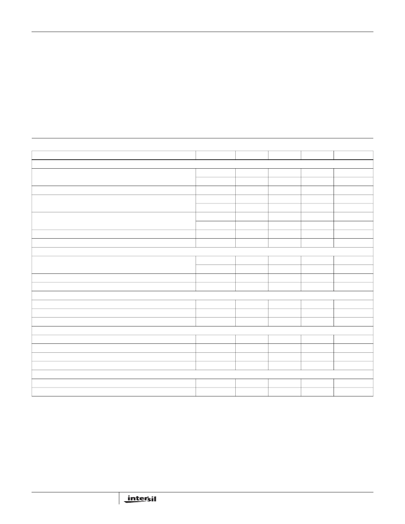
Absolute Maximum Ratings
Thermal Information
Voltage Between V+ and V- Terminals . . . . . . . . . . . . . . . . . . . 40V
Differential Input Voltage . . . . . . . . . . . . . . . . . . . . . . . . . . . . . . 15V
Peak Output Current . . . . . . . . . . . . . . . . . . . . . . . . . . . . . . . . 50mA
Operating Conditions
Temperature Range
HA-2515-5 . . . . . . . . . . . . . . . . . . . . . . . . . . . . . . . . 0
o
C to 75
o
C
Thermal Resistance (Typical, Note 1)
PDIP Package . . . . . . . . . . . . . . . . . . .
Maximum Junction Temperature (Plastic Package) . . . . . . . 150
o
C
Maximum Storage Temperature Range . . . . . . . . . -65
o
C to 150
o
C
Maximum Lead Temperature (Soldering 10s). . . . . . . . . . . . 300
o
C
θ
JA
(
o
C/W)
120
θ
JC
(
o
C/W)
N/A
CAUTION: Stresses above those listed in “Absolute Maximum Ratings” may cause permanent damage to the device. This is a stress only rating and operation of the
device at these or any other conditions above those indicated in the operational sections of this specification is not implied.
NOTE:
1.
θ
JA
is measured with the component mounted on a low effective thermal conductivity test board in free air. See Tech Brief TB379 for details.
Electrical Specifications
V
SUPPLY
=
±
15V
PARAMETER
TEMP (
o
C)
MIN
TYP
MAX
UNITS
INPUT CHARACTERISTICS
Offset Voltage
25
Full
Full
25
Full
25
Full
25
Full
-
-
-
-
-
-
-
5
-
10
14
-
250
500
50
100
-
-
mV
mV
μ
V/
o
C
nA
nA
nA
nA
M
V
Offset Voltage Average Drift
Bias Current
30
125
-
20
-
100
-
Offset Current
Input Resistance (Note 2)
Common Mode Range
TRANSFER CHARACTERISTICS
Large Signal Voltage Gain (Notes 3, 6)
40
±
10.0
25
Full
Full
25
7.5
5
74
-
15
-
90
12
-
-
-
-
kV/V
kV/V
dB
MHz
Common Mode Rejection Ratio (Note 4)
Gain Bandwidth Product (Note 5)
OUTPUT CHARACTERISTICS
Output Voltage Swing (Note 3)
Output Current (Note 6)
Full Power Bandwidth (Notes 6, 11)
TRANSIENT RESPONSE
Rise Time (Notes 3, 7, 8, 9)
Overshoot (Notes 3, 7, 8, 9)
Slew Rate (Notes 3, 7, 9, 12)
Settling Time to 0.1% (Notes 3, 7, 9, 12)
POWER SUPPLY CHARACTERISTICS
Supply Current
Power Supply Rejection Ratio (Note 10)
NOTES:
2. This parameter value is based on design calculations.
3. R
L
= 2k
.
4. V
CM
=
±
10V
5. A
V
>10.
6. V
O
=
±
10V.
7. C
L
= 50pF.
8. V
O
=
±
200mV.
9. See Transient Response Test Circuits and Waveforms.
10.
V =
±
5V.
11. Full Power Bandwidth guaranteed based on slew rate measurement using: FPBW = Slew Rate/2
π
V
PEAK
.
12. V
OUT
=
±
5V.
Full
25
25
±
10.0
±
10
600
±
12.0
±
20
1000
-
-
-
V
mA
kHz
25
25
25
25
-
-
25
25
±
60
0.25
50
50
-
-
ns
%
V/
μ
s
μ
s
±
40
-
25
Full
-
4
90
6
-
mA
dB
74
HA-2515
相关PDF资料 |
PDF描述 |
|---|---|
| HA3-2515-5 | 12MHz, High Input Impedance, Operational Amplifier |
| HA-2540 | 400MHz, Fast Settling Operational Amplifier(400MHz、快速稳定运算放大器) |
| HA-2541883 | Wideband, Fast Settling, Unity Gain Stable, Operational Amplifier |
| HA-2544883 | Video Operational Amplifier |
| HA-2556 | 57MHz, Wideband, Four Quadrant,Voltage Output Analog Multiplier(57MHz,宽频,四象限,电压输出模拟乘法器) |
相关代理商/技术参数 |
参数描述 |
|---|---|
| HA2-5151/883 | 制造商:Harris Corporation 功能描述: |
| HA2-5151-2 | 制造商:Rochester Electronics LLC 功能描述:- Bulk |
| HA2-5151-5 | 制造商:Rochester Electronics LLC 功能描述:- Bulk |
| HA2-5151-7 | 制造商:未知厂家 制造商全称:未知厂家 功能描述:Voltage-Feedback Operational Amplifier |
| HA2-5152/883 | 制造商:Rochester Electronics LLC 功能描述:- Bulk |
发布紧急采购,3分钟左右您将得到回复。