参数资料
| 型号: | HA4600CPZ |
| 厂商: | Intersil |
| 文件页数: | 3/7页 |
| 文件大小: | 0K |
| 描述: | IC VIDEO BUFFER 480MHZ 8-DIP |
| 标准包装: | 1,000 |
| 应用: | 缓冲器 |
| 电路数: | 1 |
| -3db带宽: | 480MHz |
| 转换速率: | 1770 V/µs |
| 电流 - 电源: | 10.5mA |
| 电流 - 输出 / 通道: | 20mA |
| 电压 - 电源,单路/双路(±): | ±4.5 V ~ 5.5 V |
| 安装类型: | 通孔 |
| 封装/外壳: | 8-DIP(0.300",7.62mm) |
| 供应商设备封装: | 8-PDIP |
| 包装: | 管件 |
3
FN3990.9
April 25, 2013
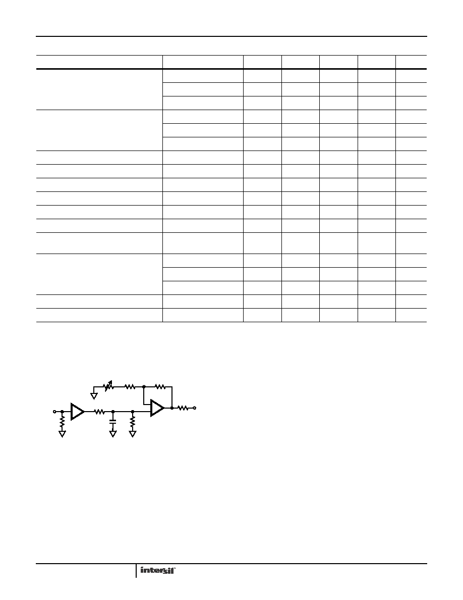
AC Test Circuit
NOTE: CL = CX + Test Fixture Capacitance.
PC Board Layout
The frequency response of this circuit depends greatly on the
care taken in designing the PC board. The use of low
inductance components such as chip resistors and chip
capacitors is strongly recommended, while a solid ground
plane is a must!
Attention should be given to decoupling the power supplies.
A large value (10
μF) tantalum in parallel with a small value
(0.1
μF) chip capacitor works well in most cases.
Keep input and output traces as short as possible, because
trace inductance and capacitance can easily become the
performance limiting items.
-3dB Bandwidth
RS =82Ω, CL = 10pF
25
-
480
-
MHz
RS =43Ω, CL = 15pF
25
-
380
-
MHz
RS =36Ω, CL = 21pF
25
-
370
-
MHz
±0.1dB Flat Bandwidth
RS =82Ω, CL = 10pF
25
-
250
-
MHz
RS =43Ω, CL = 15pF
25
-
175
-
MHz
RS =36Ω, CL = 21pF
25
-
170
-
MHz
Input Resistance
Full
200
400
-
k
Ω
Input Capacitance
Full
-
1.0
-
pF
Enabled Output Resistance
Full
-
15
-
Ω
Disabled Output Capacitance
VEN = 0.8V
Full
-
2.0
-
pF
Differential Gain (Note 3)
4.43MHz
25
-
0.01
0.02
%
Differential Phase (Note 3)
4.43MHz
25
-
0.01
0.02
Degrees
Off Isolation
1VP-P, 100MHz,
VEN = 0.8V, RL =10Ω
Full
-
85
-
dB
Slew Rate (1.5VP-P, +SR/-SR)
RS =82Ω, CL = 10pF
25
-
1750/1770
-
V/
μs
RS =43Ω, CL = 15pF
25
-
1460/1360
-
V/
μs
RS =36Ω, CL = 21pF
25
-
1410/1360
-
V/
μs
Total Harmonic Distortion (Note 3)
Full
-
0.01
0.1
%
Disabled Output Resistance
Full
-
12
-
M
Ω
NOTE:
6. This parameter is not tested. The limits are guaranteed based on lab characterization, and reflect lot-to-lot variation.
Electrical Specifications VSUPPLY = ±5V, RL = 10kΩ, VEN = 2.0V, Unless Otherwise Specified (Continued)
PARAMETER
TEST CONDITIONS
TEMP. (°C)
MIN
TYP
MAX
UNITS
500
Ω
400
Ω
510
Ω
75
Ω
VOUT
VIN
75
Ω
RS
HA4600
HFA1100
+
-
CX
10k
Ω
HA4600
相关PDF资料 |
PDF描述 |
|---|---|
| MAX5721EUA+T | IC DAC 10BIT DUAL LP SER 8-UMAX |
| VE-B5F-MX-S | CONVERTER MOD DC/DC 72V 75W |
| VE-B3L-MX-S | CONVERTER MOD DC/DC 28V 75W |
| VE-BNP-MU-F2 | CONVERTER MOD DC/DC 13.8V 200W |
| MAX5259EEE+T | IC DAC 8BIT OCTAL 3V 16-QSOP |
相关代理商/技术参数 |
参数描述 |
|---|---|
| HA-461 | 制造商:未知厂家 制造商全称:未知厂家 功能描述:CRYSTAL CLOCK OSCILLATORS |
| HA-467 | 制造商:未知厂家 制造商全称:未知厂家 功能描述:CRYSTAL CLOCK OSCILLATORS |
| HA-469 | 制造商:未知厂家 制造商全称:未知厂家 功能描述:CRYSTAL CLOCK OSCILLATORS |
| HA-46A | 制造商:未知厂家 制造商全称:未知厂家 功能描述:CRYSTAL CLOCK OSCILLATORS |
| HA-46B | 制造商:未知厂家 制造商全称:未知厂家 功能描述:CRYSTAL CLOCK OSCILLATORS |
发布紧急采购,3分钟左右您将得到回复。